Potentiostatic Electrodeposition of Ni Nanowire Arrays: A Comprehensive Guide from Synthesis to Advanced Applications
This article provides a thorough examination of the potentiostatic electrodeposition method for synthesizing nickel (Ni) nanowire arrays, a critical technique for developing advanced nanostructured materials.
Potentiostatic Electrodeposition of Ni Nanowire Arrays: A Comprehensive Guide from Synthesis to Advanced Applications
Abstract
This article provides a thorough examination of the potentiostatic electrodeposition method for synthesizing nickel (Ni) nanowire arrays, a critical technique for developing advanced nanostructured materials. Aimed at researchers and scientists, it covers foundational principles, detailed methodologies for creating high-aspect-ratio structures, and strategies for troubleshooting common experimental issues. Furthermore, it explores the validation of nanowire properties and their diverse applications in cutting-edge fields such as electrocatalysis for hydrogen evolution and biomedicine, highlighting their significance in developing sustainable energy solutions and innovative therapeutic platforms.
Principles and Potentials: Understanding Ni Nanowire Arrays and Electrodeposition Fundamentals
Definition and Fundamental Concepts
Nanowires are one-dimensional nanostructures characterized by a diameter constrained to tens of nanometers or less, with an unrestricted length, resulting in a high aspect ratio (length-to-diameter ratio) [1]. This unique geometry places them in the category of quantum wires, where quantum mechanical effects become significant due to nanoscale confinement [1]. Their high surface-area-to-volume ratio and anisotropic structure are the origin of their distinctive electrical, optical, chemical, and magnetic properties, which differ markedly from their bulk or thin-film counterparts [2].
These properties are highly tunable based on the nanowire's material composition, which can include:
- Metallic (e.g., Ni, Au, Ag, Pt) [1] [3]
- Semiconducting (e.g., Si, Ga, metal oxides like ZnO, SnO₂) [2] [4]
- Insulating (e.g., TiO₂, SiO₂) [1]
The versatility in material selection, combined with precise control over morphology, enables the engineering of nanowires for a vast array of technological applications, from nanoelectronics and energy conversion to sensing and biomedicine [1] [2].
Unique Properties of Nanowires
The transition from bulk materials to one-dimensional nanostructures imparts several unique properties.
- Quantum Confinement Effects: When the nanowire diameter approaches the de Broglie wavelength of electrons, quantum confinement occurs, leading to discrete energy levels. This can significantly alter electronic and optical properties, enabling phenomena not observed in bulk materials [2].
- Anisotropic Properties: Their elongated shape induces anisotropy, meaning properties differ along the axial direction compared to the transverse direction. This is particularly evident in magnetic nanowires, which exhibit magnetic anisotropy along the wire axis [3] [2].
- High Surface-to-Volume Ratio: This is a defining characteristic that makes nanowires exceptionally efficient for surface-dependent processes, such as catalytic reactions, gas sensing, and biomolecular binding [1] [4].
- Tunable Physical Properties: Key properties, including electrical conductivity, thermal conductivity, and mechanical strength, can be tailored by varying the nanowire's diameter, length, crystallinity, and chemical composition [5] [2].
Synthesis Methods for Nanowire Arrays
A critical advancement in the field is the fabrication of ordered nanowire arrays, where nanowires are arranged in parallel, high-density configurations. Template-assisted synthesis is a predominant method for achieving this, with several techniques available.
Diagram 1: Classification of common nanowire synthesis methods, highlighting template-assisted electrodeposition.
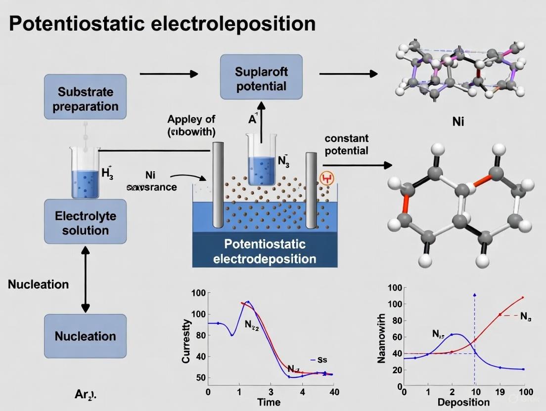
Potentiostatic Electrodeposition into Nanoporous Templates
This protocol details the synthesis of Ni nanowire arrays using potentiostatic electrodeposition, a highly controlled bottom-up method.
Experimental Protocol: Potentiostatic Electrodeposition of Ni Nanowire Arrays
Principle: A nanoporous template acts as a scaffold to confine the growth of nanowires. A metal film is first deposited on one side of the template to serve as a working electrode. When a constant cathodic potential is applied in an electrolyte containing the desired metal ions, reduction occurs at the electrode surface, initiating growth at the pore bottoms and proceeding until the pores are filled [6] [3] [7].
Required Materials:
- Template: Anodized Aluminum Oxide (AAO) membrane (e.g., 6-70 µm thickness, 40-100 nm pore diameter) [6] [3].
- Working Electrode Substrate: Sputtered Au or Cu layer (~100-200 nm) on one side of the template [7].
- Electrolyte: Nickel sulfamate or Watts bath solution containing Ni²⁺ ions [3].
- Counter Electrode: Pt mesh or foil.
- Reference Electrode: Ag/AgCl or Saturated Calomel Electrode (SCE).
- Potentiostat: For applying controlled potential.
Step-by-Step Procedure:
- Template Preparation: Select an AAO template with the desired pore diameter. Sputter a continuous, conductive Au layer (~150 nm) onto one side of the template to create the cathode [7].
- Electrochemical Cell Setup: Assemble a three-electrode cell. Mount the template with the Au-coated side facing the electrolyte and connect it as the working electrode. Place the counter and reference electrodes appropriately.
- Solution Deaeration: Purge the electrolyte with an inert gas (e.g., N₂ or Ar) for 15-20 minutes to remove dissolved oxygen.
- Potentiostatic Electrodeposition: Apply a constant cathodic potential. Typical potentials for Ni deposition range from -1.0 V to -1.8 V vs. a reference electrode [8]. The deposition process continues until the pores are filled, which can be monitored by the charge passed.
- Termination and Rinsing: Stop the electrodeposition and carefully remove the template composite from the cell. Rinse thoroughly with deionized water to remove residual electrolyte.
- Post-Processing (Optional): To obtain freestanding nanowires, the AAO template can be dissolved in a NaOH solution (e.g., 1-3 M), or a polycarbonate template can be dissolved in dichloromethane [7].
Key Parameters Influencing Nanowire Properties:
- Applied Potential: Modifies deposition rate, composition for alloys, and morphology [8].
- Template Pore Diameter: Directly determines nanowire diameter [6] [3].
- Electrolyte Composition and pH: Affects deposition efficiency and material quality [8].
- Temperature: Influences ion transport and crystallization kinetics.
Comparison of Synthesis Methods
Table 1: Comparative analysis of common nanowire synthesis methods.
| Method | Crystal Quality | Scalability | Processing Time | Temperature | Relative Cost | Key Applications |
|---|---|---|---|---|---|---|
| Potentiostatic Electrodeposition [5] [2] [7] | Moderate (Polycrystalline) | High | Short (Minutes to Hours) | Low (Room Temp.) | Low | Magnetic storage, sensors, catalysis |
| Vapor-Liquid-Solid (VLS) [2] | High (Single Crystal) | Medium | Medium (Minutes to Hours) | High (~1000°C) | Medium to High | Electronics, photonics |
| Chemical Vapor Deposition (CVD) [2] | High | Low | Medium (Minutes to Hours) | High | High | Semiconductors, Si nanowires |
| Press-Based Nanoinfiltration (PBNI) [2] | Moderate | High | Short (<1 Hour) | Material Melting Point | Low | Thermoelectrics, low-melt-point alloys |
| Solution-Liquid-Solid (SLS) [2] | Moderate | Medium | Long (Hours) | Medium (200-350°C) | Low | Colloidal semiconductor nanorods |
Quantitative Data on Nanowire Properties
The properties of nanowires are highly dependent on their synthesis conditions and geometric parameters.
Table 2: Influence of synthesis parameters on the magnetic properties of Ni and FeCoNi nanowire arrays.
| Material & Diameter | Synthesis Parameter | Key Property Changes | Explained by |
|---|---|---|---|
| Ni NWs (70 nm) [3] | Optimized electrodeposition into PAAMs | Coercivity (Hc) > 750 Oe; Squareness (Mr/Ms) = 0.65 | High density and preferred crystal orientation [(220) texture] |
| Ni NWs (80 nm) [6] | Length increased to 15 µm (Aspect ratio ~188) | Optimal Field Enhancement Factor (β) = 3686 | High aspect ratio enhancing local electric fields |
| FeCoNi NWs (40 nm) [8] | More cathodic potential (-1.0 V to -1.8 V) | Hc and Squareness increased with potential | Weakened dipolar interactions due to low membrane porosity |
| FeCoNi NWs (100 nm) [8] | More cathodic potential (-1.0 V to -1.8 V) | Hc and Squareness decreased with potential | Increased dipolar interactions between larger nanowires |
The Scientist's Toolkit: Research Reagent Solutions
Table 3: Essential materials and reagents for template-assisted electrodeposition of nanowires.
| Reagent / Material | Function / Role | Examples & Specifications |
|---|---|---|
| AAO Template [6] [7] | Defines nanowire diameter, length, and arrangement; provides growth confinement. | Pore diameter: 20-450 nm; Thickness: 1-70 µm; Pore density: 10⁹-10¹¹ cm⁻² |
| Polymer Track Membrane [8] [7] | A flexible alternative template for nanowire growth. | Polycarbonate, ~5-50 µm thick, pore diameter 10-500 nm. |
| Conductive Layer (Sputtered) [7] | Serves as the cathode for electrodeposition, sealing one end of the pores. | Gold (Au), ~100-200 nm thick; also Silver (Ag) or Copper (Cu). |
| Metal Salt Electrolyte [8] [3] | Provides the metal ions (Mⁿ⁺) for reduction and deposition into the template pores. | NiSO₄, Ni sulfamate, or mixed salts for alloys (e.g., Fe, Co, Ni). |
| Potentiostat | Apparatus that applies a constant potential vs. a reference electrode to control the reduction reaction. | Applied potential range: typically -1.0 V to -2.0 V (vs. Ag/AgCl/SCE). |
Application Notes in Research and Development
The unique properties of nanowires make them critical components in advanced research and development.
Magnetic Storage and Memory: Arrays of magnetic nanowires (e.g., Ni, FeCoNi) are prime candidates for building 3D magnetic racetrack memories and high-density recording media. Their magnetic anisotropy allows for the stabilization of magnetic domains along the wire axis, enabling dense data storage [8] [3]. The coercivity and squareness of the arrays can be tuned by varying the nanowire diameter, length, and inter-wire distance to control magnetostatic interactions [8].
Biosensing and Therapeutics: Nanowires functionalized with biorecognition elements (antibodies, DNA) are used in highly sensitive biosensors. Their high surface area allows for excellent biomarker binding, enabling the detection of viruses, DNA, and neurotransmitters. Silicon nanowire field-effect transistors (FETs) can detect binding events as conductance changes, offering label-free detection [1] [9].
Energy Conversion and Storage: Nanowires play a significant role in batteries, water splitting, and thermoelectrics. For instance, Ni nanowire arrays with ultra-high aspect ratios serve as efficient electrocatalysts for the hydrogen evolution reaction (HER) due to their large surface area [5]. Metal oxide nanowires are also explored as advanced electrode materials to improve battery performance and cycle life [5].
Field Emitters and Electronics: The sharp tips and high aspect ratios of nanowires, such as Ni arrays, make them excellent field emitters. They can emit electrons at low turn-on fields, which is valuable for display technologies and vacuum microelectronics [6].
Potentiostatic electrodeposition stands as a pivotal synthesis technique for fabricating nickel (Ni) nanowire arrays, a material system with significant applications in fields ranging from data storage to electrocatalysis. This method offers superior control over the electrochemical driving force compared to its galvanostatic counterpart, enabling precise manipulation of nanowire composition, microstructure, and consequently, their functional properties. Within the context of a broader thesis on advanced nanomaterials, this document serves as a detailed Application Note and Protocol, providing researchers and scientists with a comprehensive guide to the potentiostatic electrodeposition mechanism for Ni nanowire arrays. It synthesizes current research findings, presents quantitative data in an accessible format, and outlines standardized experimental methodologies to ensure reproducibility and reliability in nanomaterial synthesis.
Core Mechanism and Principle
Potentiostatic electrodeposition is an electrode reaction process controlled by a constant applied potential. In the context of nanowire synthesis, it involves the electrochemical reduction of metal ions from an electrolyte solution and their deposition into the nanochannels of a template. The fixed potential directly governs the nucleation and growth kinetics at the working electrode surface. This precise control is crucial for achieving uniform, dense nanowire arrays with tailored magnetic and catalytic properties.
The process begins when a cathodic potential is applied between a working electrode (the template with a conductive backing) and a counter electrode. Nickel ions (Ni²⁺) in the electrolyte migrate towards the cathode under the influence of the electric field. Upon reaching the cathode surface within the pores, they gain electrons and are reduced to metallic nickel (Ni⁰), initiating nucleation and subsequent one-dimensional growth along the pore length. The potentiostatic mode is particularly advantageous for producing segmented nanowires or alloys from a single electrolyte bath, as the applied potential can be precisely switched or maintained to control the composition and structure of the deposited material [10].
Diagram 1: Potentiostatic electrodeposition mechanism for Ni nanowire formation.
The properties of electrodeposited Ni nanowires are highly sensitive to synthesis parameters. The following tables consolidate key quantitative data from recent research, providing a reference for the expected outcomes and their dependence on experimental conditions.
Table 1: Influence of Electrodeposition Potential on Nanowire Properties
| Material System | Applied Potential (V vs. Ag/AgCl) | Key Outcome | Reference |
|---|---|---|---|
| FeNi Nanowires | -1.0 to -2.0 | Ni content increases with more negative potential | [10] |
| FeCo Nanowires | -1.0 to -2.0 | Weak sensitivity of chemical composition to potential | [10] |
| Ni Nanowires | -2.0 and lower | Investigation of long-term, high negative overvoltages | [11] |
Table 2: Magnetic Properties of Ni Nanowire Arrays
| Nanowire Diameter (nm) | Aspect Ratio (Length/Diameter) | Coercivity, Hc (Oe) | Squareness (Mr/Ms) | Reference |
|---|---|---|---|---|
| 70 | ~100 (Length: 6-12 μm) | >750 | 0.65 | [12] |
| 100 | 12,000 (Length: 12 μm) | - | Reported for RRAM devices | [13] |
| 100 | ~3,200 (Length: 320 μm) | 550 | 0.80 | [14] |
Table 3: Electrolyte Compositions for Potentiostatic Electrodeposition
| Component | Concentration Range | Function | Example System |
|---|---|---|---|
| NiSO₄·6H₂O | 0.06 - 0.5 M | Primary source of Ni²⁺ ions | Ni NW in AAO [12] [14] |
| NiCl₂·6H₂O | ~0.1 M | Improves anode dissolution, enhances conductivity | Ni NW in AAO [12] |
| H₃BO₃ | 0.4 - 0.5 M | Buffering agent, stabilizes pH at the cathode interface | Ni, FeNi, FeCo NW [12] [10] [14] |
| Ascorbic Acid | ~0.003 M | Antioxidant, prevents oxidation of Fe²⁺ in related systems | FeCo/FeNi NW [10] |
Detailed Experimental Protocols
Template Preparation and Electrode Assembly
Objective: To create a nano-porous template with a conductive working electrode for nanowire growth.
Materials:
- Porous Anodic Alumina Membrane (PAAM) or Polycarbonate Membrane.
- Aluminum foil (high purity, 99.995%) for self-made PAAM [12] [11].
- Sputtering system (e.g., for E-beam evaporation).
- Conductive metal targets (e.g., Cu, Au, Ti).
- Electrolytes for anodization (e.g., oxalic acid, sulfuric acid).
Procedure:
- Template Fabrication/Selection: Use commercially available track-etched polycarbonate membranes (e.g., 100 nm pore diameter, 6 μm thickness) [10] or fabricate PAAM via a two-step anodization process [12] [11]. For PAAM, anodize high-purity Al foil at a constant voltage (e.g., 30-40 V) in a suitable acid electrolyte (e.g., 5% oxalic acid).
- Barrier Layer Removal: For PAAM, chemically etch the insulating aluminum oxide barrier layer at the pore bottom. This is typically done by immersion in 8 wt.% phosphoric acid at room temperature [14].
- Working Electrode Preparation: Deposit a continuous conductive metal layer (e.g., Cu, ~450 nm or Au) onto one side of the template using electron-beam sputtering or thermal evaporation [12] [13]. This layer acts as the cathode for electrodeposition and must seal the pores at one end.
Electrolyte Preparation and Cell Setup
Objective: To prepare a stable, homogeneous electrolyte and assemble the electrochemical cell.
Materials:
- Nickel Sulfate Hexahydrate (NiSO₄·6H₂O)
- Boric Acid (H₃BO₃)
- Deionized Water (Resistivity >18 MΩ·cm)
- pH meter and adjusters (e.g., H₂SO₄, NaOH)
- Three-electrode electrochemical cell
Procedure:
- Electrolyte Formulation: Dissolve the appropriate salts in deionized water to achieve the desired concentration. A typical Watt's nickel bath might contain 0.5 M NiSO₄ and 0.4 M H₃BO₃ [14]. For alloy systems like FeNi, add corresponding metal salts (e.g., FeSO₄, NiSO₄) and antioxidants (e.g., ascorbic acid) [10].
- pH Adjustment: Adjust the solution pH to an optimal range (e.g., 3.0-4.0) using dilute sulfuric acid or sodium hydroxide [10] [14].
- Cell Assembly: Assemble a three-electrode cell.
- Working Electrode (WE): The template with the sputtered conductive layer.
- Counter Electrode (CE): A platinum mesh or nickel plate.
- Reference Electrode (RE): Ag/AgCl (or Saturated Calomel Electrode, SCE). Ensure the conductive side of the template (WE) faces the counter electrode.
Potentiostatic Electrodeposition and Post-Processing
Objective: To execute the controlled growth of Ni nanowires and retrieve the final product.
Materials:
- Potentiostat (e.g., AUTOLAB PGSTAT302N)
- Magnetic stirrer
- Fume hood
- NaOH solution (e.g., 5 M)
Procedure:
- Solution Degassing and Pore Wetting: Prior to deposition, degas the electrolyte by bubbling with an inert gas (e.g., N₂). To ensure complete pore filling, immerse the template in the electrolyte under reduced pressure to remove trapped air [14].
- Potentiostatic Deposition: Place the assembled cell in a temperature-controlled environment (e.g., 20-40°C). Apply a constant cathodic potential to the working electrode. Typical deposition potentials for Ni range from -1.0 V to -2.0 V vs. Ag/AgCl [10] [14]. Monitor the chronoamperometric (current-time) response.
- Process Termination: The deposition is complete when the pores are filled, often indicated by a sharp increase in cathodic current as a continuous metal film forms over the template surface [10].
- Post-Processing:
- Rinsing: Carefully remove the template and rinse thoroughly with deionized water to remove residual electrolyte.
- Template Removal: Dissolve the template matrix to liberate the nanowires. For alumina templates (PAAM), immerse in 5 M NaOH solution [14]. For polycarbonate, use organic solvents like dichloromethane.
- Characterization: The resulting nanowire arrays can be characterized using Scanning Electron Microscopy (SEM), X-ray Diffraction (XRD), and Vibrating Sample Magnetometry (VSM).
Diagram 2: Experimental workflow for synthesizing Ni nanowire arrays.
The Scientist's Toolkit: Research Reagent Solutions
Table 4: Essential Materials for Potentiostatic Electrodeposition of Ni Nanowires
| Item Name | Function/Brief Explanation | Typical Specification/Example |
|---|---|---|
| Porous Anodic Alumina (PAAM) Template | Provides a rigid scaffold with parallel nanochannels to define the nanowire diameter and arrangement. | Pore diameter: 70-100 nm; Thickness: 6-75 μm [12] [13]. |
| Polycarbonate Track-Etch Membrane | An alternative template offering greater inter-pore distance, reducing magnetostatic interactions between nanowires [10]. | Pore diameter: 100 nm; Thickness: 6 μm; Porosity: ~3% [10]. |
| Nickel Sulfate (NiSO₄·6H₂O) | The primary source of Ni²⁺ ions in the electrolyte for the electrochemical reduction and deposition. | Analytical grade; Concentration: 0.06 - 0.5 M [12] [14]. |
| Boric Acid (H₃BO₃) | A buffering agent crucial for maintaining a stable pH at the cathode-electrolyte interface, preventing the formation of basic salts and ensuring smooth deposition. | Analytical grade; Concentration: 0.4 - 0.5 M [12] [14]. |
| Conductive Seed Layer (Cu, Au) | Sputtered onto the template to serve as the working electrode (cathode), providing electrical contact and initiating nanowire growth from the pore bottoms. | Thickness: ~450 nm; High continuity and adhesion [12] [13]. |
| Ascorbic Acid | An antioxidant used in alloy deposition (e.g., FeNi, FeCo) to prevent the oxidation of Fe²⁺ ions (to Fe³⁺) in the electrolyte, ensuring consistent composition [10]. | Added in small quantities (~0.003 M) [10]. |
| Potentiostat | The core instrument that applies a constant potential between the working and reference electrodes, precisely controlling the electrochemical driving force for deposition. | Capable of three-electrode measurements and accurate potential control [10]. |
| Ag/AgCl Reference Electrode | Provides a stable and known reference potential against which the working electrode potential is precisely controlled and measured. | - |
| Sodium Hydroxide (NaOH) Solution | Used post-deposition to chemically dissolve the alumina template (PAAM) without significantly attacking the Ni nanowires, freeing them for analysis or application. | 1-5 M solution [14] [13]. |
Template-assisted synthesis, utilizing Anodic Aluminum Oxide (AAO) and track-etched polycarbonate (PC) membranes, is a foundational technique for fabricating one-dimensional nanoscale materials. This method provides unparalleled control over the geometry of nanostructures such as nanowires and nanotubes, which is critical for tailoring their physical properties. This Application Note details the comparative advantages of these templates and provides a standardized protocol for the potentiostatic electrodeposition of Ni nanowire arrays, a key material for applications in hard magnetism and electrocatalysis. The procedures are contextualized within a broader research thesis on advanced nanomaterial synthesis.
Template-assisted synthesis is a versatile nanofabrication strategy where the porous structure of a membrane is used as a scaffold to dictate the shape and size of nanomaterials. The two most common templates are:
- Anodic Aluminum Oxide (AAO) Templates: Characterized by a highly ordered, honeycomb-like array of cylindrical nanopores [15] [16]. The pore dimensions, including diameter, density, and aspect ratio, can be precisely tuned by varying anodization parameters such as electrolyte type, voltage, and temperature [15] [17].
- Track-Etched Polycarbonate (PC) Membranes: These templates feature randomly distributed, cylindrical pores created by bombarding a polymer sheet with heavy ions followed by chemical etching [18] [19]. While lacking the periodicity of AAO, they offer commercial availability with very small pore diameters (down to ~10 nm) and are easily processed [18].
This note explores the advantages of these templates and standardizes their use in synthesizing high-aspect-ratio metallic nanowires.
Comparative Analysis: AAO vs. Polycarbonate Membranes
The choice of template is dictated by the specific requirements of the target application. Below is a quantitative comparison of their key characteristics.
Table 1: Key Characteristics of AAO and Polycarbonate Templates
| Feature | Anodic Aluminum Oxide (AAO) | Track-Etched Polycarbonate (PC) |
|---|---|---|
| Pore Arrangement | Highly ordered, hexagonal close-packing [15] | Random, non-ordered [18] |
| Typical Pore Diameter | 25 - 200 nm [16] [17] | 15 - 200 nm [18] |
| Aspect Ratio (Pore Depth/Diameter) | Very high (e.g., >3000) [16] | Moderate (e.g., 50 - 400) [18] |
| Surface Chemistry | Alumina (Al₂O₃), hydrophilic | Polycarbonate, can be hydrophilic or hydrophobic |
| Template Rigidity | Rigid and brittle | Flexible |
| Primary Advantage | High order and uniformity; extreme aspect ratios | Commercial availability; very small pore sizes; ease of processing |
Application-Specific Advantages
AAO for High-Performance Magnetic and Electrocatalytic Nanowires
The high aspect ratio and regularity of AAO templates make them ideal for applications relying on shape anisotropy and large surface area.
- Uniaxial Magnetization: Ni nanowires electrodeposited into high-aspect-ratio AAO pores (e.g., 100 nm diameter, 320 µm length, aspect ratio 3200) exhibit superior hard magnetic properties. Research shows these arrays achieve a high coercivity of 550 Oe and a magnetic squareness ratio of up to 0.8, with the easy magnetization axis aligned with the nanowire length [16].
- Enhanced Electrocatalysis: The extremely large surface area of Ni nanowire arrays fabricated via AAO templates significantly boosts their electrocatalytic performance for reactions like the hydrogen evolution reaction (HER). Studies demonstrate a reduction in hydrogen overvoltage of almost 0.2 V and a dramatic increase in current density compared to planar Ni films [16].
Polycarbonate for Versatile Nanomaterial Fabrication
PC membranes are widely used for their simplicity and effectiveness in producing a diverse range of nanomaterials.
- Versatile Nanostructure Synthesis: The uniform cylindrical pores are excellent templates for producing not only metallic nanowires (e.g., Cu, Ni) but also conductive polymer nanotubules and superconducting nanowires [20] [18]. Their commercial availability accelerates research and development.
- Fundamental Growth Studies: The transient current during potentiostatic electrodeposition into PC membranes can be divided into distinct stages, providing insight into the growth dynamics and mass transfer limitations within nanoscale pores [18].
Experimental Protocol: Potentiostatic Electrodeposition of Ni Nanowire Arrays using AAO Templates
This protocol is optimized for the synthesis of high-aspect-ratio Ni nanowires with superior magnetic and catalytic properties, as referenced in the thesis context.
The Scientist's Toolkit: Essential Research Reagents
Table 2: Key Reagents and Materials for Ni Nanowire Synthesis
| Item | Function / Specification | Experimental Role |
|---|---|---|
| High-Purity Aluminum Foil | Substrate for AAO template (≥99.7%) [16] | Serves as the starting material for the two-step anodization process. |
| Oxalic Acid (H₂C₂O₄) | Electrolyte for anodization (e.g., 0.6 mol/L) [16] | Forms the self-ordered nanoporous AAO structure. |
| Nickel Sulfate (NiSO₄) | Metal ion source for electrodeposition (e.g., 0.5 M) [16] | Provides Ni²⁺ cations for reduction into metallic nanowires. |
| Boric Acid (H₃BO₃) | Buffering agent in plating bath (e.g., 0.4 M) [16] | Maintains stable pH to prevent hydroxide formation during deposition. |
| Phosphoric Acid (H₃PO₄) | Pore-widening and barrier layer etching agent (e.g., 5-8 wt.%) [16] [17] | Used to selectively etch the AAO, opening pores and removing the barrier layer. |
| Sputtered Copper Layer | Conductive working electrode | Applied to one side of the AAO template to serve as the cathode for electrodeposition. |
Workflow Diagram: Ni Nanowire Array Fabrication
The following diagram illustrates the multi-step fabrication process for creating Ni nanowire arrays via template-assisted electrodeposition.
Step-by-Step Procedure
Part A: Synthesis of AAO Template [16] [15]
- Substrate Preparation: Mechanically and electrochemically polish a high-purity aluminum substrate to a mirror finish to ensure a uniform starting surface.
- First Anodization: Perform anodic oxidation in a 0.6 mol/L oxalic acid solution at a constant voltage (e.g., 90 V) and low temperature (<10 °C to prevent dissolution) for several hours. This creates an initial, imperfect porous layer.
- Oxide Removal: Dissolve the initial oxide layer in a mixture of chromic and phosphoric acid, revealing a patterned aluminum surface with ordered concavities.
- Second Anodization: Re-anodize the sample under the same conditions as Step 2. This results in a highly ordered AAO film with straight, parallel nanopores. The pore length is controlled by the anodization time.
- Barrier Layer Etching & Release: Immerse the AAO film in a phosphoric acid solution (e.g., 5-8 wt.%) to remove the barrier layer at the pore bottom and slightly widen the pores. For freestanding templates, the remaining aluminum substrate is selectively dissolved.
Part B: Electrodeposition of Ni Nanowires [16] [18]
- Electrode Preparation: Sputter a thin conductive metal layer (e.g., Cu) onto one side of the AAO template to act as the working electrode/cathode.
- Electrolyte Infiltration: Place the template in the electroplating solution (0.5 M NiSO₄ + 0.4 M H₃BO₄, pH 4.0) under reduced pressure to ensure complete filling of the nanopores.
- Potentiostatic Electrodeposition: Assemble a standard three-electrode cell (Ni counter electrode, Ag/AgCl reference electrode). Apply a constant negative potential to initiate and sustain the reduction of Ni²⁺ ions to metallic Ni within the pores. The growth process can be monitored by tracking the transient cathodic current.
- Harvesting Nanowires: After deposition, dissolve the AAO template in a 5 M NaOH solution to liberate the embedded Ni nanowire array.
Both AAO and polycarbonate membranes are indispensable tools in the nanofabrication toolkit. The choice between them hinges on the specific needs of the research: AAO templates are superior for applications demanding high aspect ratios, perfect uniformity, and superior collective properties like enhanced magnetization and electrocatalysis. In contrast, polycarbonate membranes offer a flexible and accessible platform for rapidly producing nanomaterials where extreme pore order is not critical. The provided protocol for Ni nanowire synthesis via AAO templates establishes a reliable foundation for advancing research in nanomagnetism and energy conversion.
Within the field of nanotechnology, nickel (Ni) nanowires stand out as a subject of intensive research due to their distinctive one-dimensional (1D) structure and the resultant properties. This application note details the key material properties of Ni nanowires, with a specific focus on the interplay between their structural, magnetic, and electrocatalytic characteristics. Framed within a broader thesis on potentiostatic electrodeposition, this document provides a consolidated resource for researchers and scientists, featuring structured quantitative data, detailed experimental protocols, and essential reagent information to facilitate the replication and advancement of research in this domain.
Structural and Magnetic Properties
The properties of Ni nanowires are profoundly influenced by their structural characteristics, which are in turn controlled by the parameters of the template-assisted electrodeposition process.
Influence of Deposition Potential on Structure and Magnetism
The working electrode potential during electrodeposition is a critical factor that directly impacts the crystalline structure and magnetic configuration of the resulting Ni nanowires. Studies have shown that varying the deposition potential can trigger a transition from a 3-dimensional Imry and Ma random anisotropy type to a cooperative quasi-1-dimensional superspin type magnetic configuration [21]. This transition is linked to changes in structural factors sensitive to the deposition potential, such as crystalline texture, grain size, and grain shape [21].
Influence of Geometric and Packing Parameters
The geometry of the nanowires and their arrangement within the array are equally pivotal. Aspect ratio (length/diameter) and packing factor (volume fraction of nanowires in the membrane) are two key geometric parameters.
- High Aspect Ratio: Ni nanowires with an ultra-high aspect ratio (e.g., 700) exhibit superior magnetic properties. Research has demonstrated that increasing the aspect ratio suppresses magnetization reversal, leading to enhanced coercivity (resistance to demagnetization) and squareness (a measure of magnetic remanence) [11] [14]. For instance, arrays with an aspect ratio of 700 have shown a squareness value of up to 0.8 and a coercivity of 550 Oe, indicating strong uniaxial magnetic anisotropy with the easy axis parallel to the nanowire axis [14].
- Packing Factor: In densely packed arrays (packing factor ≥37%), magnetostatic interactions between neighboring nanowires become significant. These dipolar interactions can alter the demagnetizing field and lead to a reversal magnetization state described by a "curling"-type model [11]. This effect underscores the importance of controlling inter-wire distance for tailoring the overall magnetic response of the array.
Table 1: Summary of Magnetic Properties in Ni Nanowire Arrays
| Aspect Ratio | Packing Factor | Coercivity (Hc) | Squareness (Mr/Ms) | Easy Axis | Citation |
|---|---|---|---|---|---|
| ~700 | ≥37% | Not Specified | Not Specified | Parallel to wire axis | [11] |
| Ultra-high (e.g., 3200) | Not Specified | ~550 Oe | ~0.8 | Parallel to wire axis | [14] |
| High | Low | Not Specified | Up to 0.6 | Parallel to wire axis | [22] |
Electrocatalytic Performance
The exceptionally high surface area of Ni nanowire arrays makes them outstanding candidates for electrocatalytic applications, particularly for the hydrogen evolution reaction (HER).
Enhanced Hydrogen Evolution Reaction
Compared to flat Ni films, Ni nanowire array electrodes demonstrate significantly superior electrocatalytic performance. The ultra-high surface area provided by the nanowire morphology reduces the hydrogen overvoltage to approximately 0.1 V, which is almost 0.2 V lower than that observed on electrodeposited Ni films [14]. Consequently, the current density for hydrogen evolution is drastically increased, reaching values of about -580 A/m² at -1.0 V and -891 A/m² at -1.5 V (vs. Ag/AgCl) [14]. This performance is attributed to the large number of active sites available for the reaction on the nanowire arrays.
Table 2: Electrocatalytic Performance of Ni Nanowire Arrays for Hydrogen Evolution
| Electrode Type | Hydrogen Overvoltage | Current Density at -1.0 V | Current Density at -1.5 V | Citation |
|---|---|---|---|---|
| Ni Nanowire Array | ~0.1 V | ~ -580 A/m² | ~ -891 A/m² | [14] |
| Electrodeposited Ni Film | ~0.3 V | Not Specified | Not Specified | [14] |
Experimental Protocols
This section provides a detailed methodology for the synthesis and basic characterization of Ni nanowire arrays via potentiostatic electrodeposition, a foundational technique in this field.
Potentiostatic Electrodeposition of Ni Nanowires
Objective: To fabricate a uniform array of Ni nanowires with high aspect ratio and defined magnetic properties using an anodized aluminum oxide (AAO) template.
Materials: Refer to Section 5, "The Scientist's Toolkit," for a list of required reagents and materials.
Procedure:
AAO Template Preparation:
- Begin with an aluminum substrate (e.g., rod or foil of high purity, ≥99%) [14].
- Electrochemically polish the substrate to achieve a mirror-like surface finish [14].
- Perform a two-step anodization in an oxalic acid electrolyte (e.g., 0.3 M - 0.6 M) under potentiostatic conditions (e.g., 40 V for 45 nm pores or 90 V for 100 nm pores) at low temperature (0-10 °C) to form a highly ordered nanoporous array [23] [14].
- Remove the barrier layer by chemical etching in phosphoric acid to open the pores at the bottom [14].
- Sputter a conductive metal layer (e.g., copper or gold) onto one side of the AAO template to serve as the working electrode for electrodeposition [14].
Electrolyte Preparation:
Nanowire Electrodeposition:
- Assemble a standard three-electrode electrochemical cell, with the AAO template as the working electrode, a nickel plate as a soluble anode, and an Ag/AgCl reference electrode [14].
- Prior to deposition, fill the nanochannels with electrolyte by immersing the template under reduced pressure [14].
- Apply a constant cathodic potential (typically in the range of -1.0 V to -2.0 V vs. Ag/AgCl) to initiate and sustain the reduction of Ni²⁺ ions and nanowire growth within the pores [21] [14].
- Monitor the cathodic current; a sudden increase typically indicates the pores are completely filled and nanowires have reached the top surface [10].
Post-Deposition Processing:
- Dissolve the AAO template in a 5 M NaOH solution to liberate the Ni nanowire array [14].
- Rework the liberated nanowires thoroughly with deionized water.
Characterization:
- Structural: Use Scanning Electron Microscopy (SEM) to confirm nanowire morphology, diameter, length, and array density. Employ X-ray Diffraction (XRD) to determine crystallographic structure and preferred orientation [11] [14].
- Magnetic: Use a Vibrating Sample Magnetometer (VSM) to measure hysteresis loops with the magnetic field applied parallel and perpendicular to the nanowire axis to determine coercivity, squareness, and magnetic anisotropy [11] [14].
- Electrocatalytic: Perform electrochemical measurements in an alkaline medium (e.g., 1 M KOH) to assess hydrogen evolution reaction performance, including overpotential and Tafel slope analysis [14].
The Scientist's Toolkit
This section catalogs the essential reagents and materials required for the potentiostatic electrodeposition and characterization of Ni nanowires, as derived from the cited protocols.
Table 3: Essential Research Reagents and Materials for Ni Nanowire Synthesis
| Item | Specification / Example | Primary Function | Citation |
|---|---|---|---|
| Aluminum Substrate | High purity foil or rod (≥99.99%) | Base material for the creation of the Anodic Aluminum Oxide (AAO) template. | [11] [14] |
| Oxalic Acid | 0.3 M - 0.6 M aqueous solution | Electrolyte for the anodization process to create the nanoporous AAO template. | [23] [14] |
| Phosphoric Acid | 5-8 wt.% aqueous solution | Chemical etchant to remove the barrier layer of the AAO template, opening the pores. | [14] |
| Nickel Sulfate | 0.5 M in deposition bath | Source of Ni²⁺ ions for electrodeposition and growth of the nickel nanowires. | [14] |
| Boric Acid | 0.4 M in deposition bath | Buffer agent in the electrodeposition electrolyte to maintain a stable pH (~4.0). | [14] |
| Sodium Hydroxide | 5 M aqueous solution | Strong base used to dissolve the AAO template after electrodeposition to release the nanowires. | [14] |
| Sputtering Target | Copper or Gold | Source for depositing a conductive layer onto the AAO template to serve as the working electrode. | [14] |
Ni nanowires produced via template-assisted potentiostatic electrodeposition present a versatile and highly tunable platform for advanced materials research. Their magnetic properties, including high coercivity and squareness, can be strategically engineered by controlling the deposition potential, aspect ratio, and packing density. Simultaneously, their unique 1D morphology endows them with exceptional electrocatalytic performance, particularly for the hydrogen evolution reaction. The protocols and data summarized in this application note provide a foundational framework for researchers to explore and exploit these distinct characteristics in applications ranging from data storage and spintronics to energy conversion and catalysis.
Application Notes
Electrodeposited nickel (Ni) nanowire arrays represent a significant advancement in nanotechnology, offering unique properties due to their one-dimensional structure, high surface-to-volume ratio, and tunable magnetic and catalytic characteristics. Synthesized via template-assisted potentiostatic electrodeposition, these nanostructures are pivotal in developing next-generation devices across data storage, sensing, energy conversion, and biomedical fields. Their compatibility with scalable fabrication processes and the ability to precisely control their dimensions, composition, and crystallography make them exceptionally versatile for both fundamental research and industrial applications [5] [8].
Data Storage
The pursuit of higher data storage density is a primary driver in the development of electrodeposited magnetic Ni nanowire arrays. Their inherent uniaxial magnetic anisotropy makes them excellent candidates for building three-dimensional (3D) magnetic memory units, potentially achieving densities of several dozen terabits per square inch [8].
- 3D Racetrack Memories: This pioneering concept utilizes vertically arranged arrays of magnetic nanowires embedded in a non-magnetic matrix. Instead of storing data in a two-dimensional plane, information is encoded as magnetic domains along the length of each nanowire. Data is read and written by controlling the motion of these domain walls along the nanowires using spin-polarized currents [8].
- Tunable Magnetic Properties: The magnetic performance crucial for data storage, such as coercivity (HC) and saturation magnetization (MS), can be systematically engineered by controlling the electrodeposition parameters. Key factors include:
- Nanowire Diameter: A reduction in diameter decreases magnetostatic interactions between neighboring nanowires, generally leading to an increase in coercivity and squareness [8].
- Electrodeposition Potential: Variations in the applied cathodic potential can modify the chemical composition of alloyed nanowires (e.g., FeCoNi), directly influencing their magnetic properties. For instance, more cathodic potentials can increase Ni content, altering the coercivity [8].
- Crystallographic Texture: Electrodeposited Ni nanowires typically exhibit a face-centered cubic (fcc) structure with a preferential growth along the [111] plane, which contributes to their uniaxial magnetic anisotropy, making the axial direction the easy magnetization axis [5].
Table 1: Magnetic Properties of Electrodeposited Ni-Based Nanowires for Data Storage
| Nanowire Type | Diameter (nm) | Coercivity, HC (kA/m) | Saturation Magnetization, MS (kA/m) | Key Application | Citation |
|---|---|---|---|---|---|
| Ni Nanowires | Not Specified | Uniaxial anisotropy confirmed | Uniaxial anisotropy confirmed | 3D magnetic memory | [5] |
| FeCoNi Nanowires | 40 | Increases with applied potential | Increases with applied potential | 3D racetrack memory | [8] |
| FeCoNi Nanowires | 100 | Decreases with applied potential | Increases with applied potential | 3D racetrack memory | [8] |
Sensing and Biomedical Devices
The high surface-area-to-volume ratio of Ni nanowire arrays makes them highly sensitive transducers for chemical and biological sensing. This property allows for direct modulation of electrical or optical signals upon target binding, enabling label-free biomarker quantification [24].
- Electrochemical Immunosensors: Nanowire-based platforms can be functionalized with specific antibodies or aptamers to create highly sensitive biosensors. For example, similar principles using gold-electrodeposited platforms have been successfully applied to detect biomarkers like neutrophil-associated lipocalin (NGAL) for acute kidney injury, achieving limits of detection compatible with clinical diagnostic ranges [25].
- Hydrogen Evolution Reaction (HER) Catalysis: Ni nanowire array electrodes, fabricated by potentiostatic electrodeposition into anodized alumina templates, demonstrate exceptional electrocatalytic activity. Their extremely large surface area results in a lower overpotential and higher current density for the hydrogen evolution reaction compared to conventional electrodeposited Ni films, positioning them as efficient and cost-effective catalysts for green hydrogen production [5].
- Drug Delivery and Biomedical Imaging: While more advanced for other nanomaterials, the principles apply to functionalized Ni-based systems. Nanowires can be engineered for precise drug delivery, including heat-activated release for cancer treatment or controlled release kinetics from embedded arrays. Their functionalized surfaces can also serve as contrast agents for biomedical imaging techniques like MRI [24].
Table 2: Performance Metrics of Nanowire-Based Applications in Sensing and Energy
| Application Area | Key Performance Metric | Reported Value / Finding | Citation |
|---|---|---|---|
| Biosensing (NGAL) | Limit of Detection (LOD) | 0.56 μg/mL | [25] |
| Biosensing (NGAL) | Sensitivity | 21.8 μA mL/μg | [25] |
| HER Electrocatalysis | Performance | Lower overpotential & higher current density vs. Ni films | [5] |
| Drug Delivery | Concept Validation | Heat-activated drug release; Controlled release kinetics | [24] |
Experimental Protocols
Protocol 1: Potentiostatic Electrodeposition of Ni Nanowire Arrays
This protocol details the synthesis of high-aspect-ratio Ni nanowire arrays using template-assisted potentiostatic electrodeposition, a method prized for its versatility and scalability [8] [5].
Research Reagent Solutions
Table 3: Essential Reagents and Materials for Electrodeposition
| Item Name | Function / Explanation |
|---|---|
| Porous Template | Serves as a nanoscale mold. Typically Anodized Aluminum Oxide (AAO) or polycarbonate membranes, defining nanowire diameter and arrangement [8] [5]. |
| Electrodeposition Bath | A Watts-type bath or similar electrolyte containing Ni ions (e.g., NiSO₄, NiCl₂). Provides the source of Ni²⁺ ions for reduction and deposition into the template pores [26]. |
| Nickel Anode | A high-purity nickel plate (99.8%+) serving as the soluble anode. It maintains the ion concentration in the bath by dissolving as deposition proceeds [26]. |
| Sputtered Contact Layer | A thin, conductive metal layer (e.g., Copper or Gold) vapor-deposited on one side of the template. It acts as the working electrode cathode, closing the pores and enabling electrical contact for electrodeposition [8]. |
| Potentiostat | Instrument used to apply a constant cathodic potential (e.g., -1.0 V to -1.8 V vs. Ag/AgCl) to the working electrode, ensuring controlled nucleation and growth of the nanowires [8]. |
Methodology
The experimental workflow for the potentiostatic electrodeposition of Ni nanowires is systematic, as shown in the diagram below.
Diagram: Workflow for Electrodepositing Ni Nanowire Arrays
Step-by-Step Procedure:
- Template and Electrode Preparation: Select an AAO or polycarbonate membrane with the desired pore diameter (e.g., 40 nm or 100 nm). Sputter a thin, continuous layer of gold or copper onto one side of the template to create a conductive working electrode and seal the pores at that end [8].
- Electrochemical Cell Assembly: Assemble a standard three-electrode cell.
- Working Electrode: The template with the sputtered contact layer.
- Counter Electrode: An inert platinum or nickel wire/foil.
- Reference Electrode: An Ag/AgCl (sat. KCl) electrode. Immerse the electrodes in the Ni electroplating solution (e.g., a Watts bath containing Ni salts and boric acid) [26].
- Potentiostatic Electrodeposition: Using a potentiostat, apply a constant, optimized cathodic potential (typically between -1.0 V and -1.8 V vs. Ag/AgCl). The potential should be selected based on the desired nanowire composition, morphology, and growth rate. Monitor the current to track the deposition process [8].
- Termination and Processing: Once the deposition current indicates the template pores are fully filled (nanowires reach the desired length), terminate the potential. Carefully remove the template-electrode assembly from the solution and rinse thoroughly with deionized water.
- Template Removal (Optional): To obtain free-standing nanowire arrays, the template can be dissolved using an appropriate etchant. AAO templates are dissolved in NaOH solution, while polycarbonate membranes are dissolved in CH₂Cl₂ [8].
Protocol 2: Optimization of Electrodeposition Parameters Using the Taguchi Method
To achieve reproducible nanowires with tailored properties, systematic optimization of deposition parameters is crucial. The Taguchi method provides a robust statistical framework for this purpose, significantly reducing the number of experiments required [26].
Methodology
The optimization process is a defined cycle of design, experimentation, and analysis.
Diagram: Taguchi Method Optimization Workflow
Step-by-Step Procedure:
- Factor and Level Selection: Identify the key electrodeposition parameters (control factors) to be optimized and define the range for each. For Ni-Al₂O³ composite coatings, critical factors often include [26]:
- Current Density (e.g., 2, 3, 4, 5 A/dm²)
- Al₂O₃ Particle Concentration in the bath (e.g., 10, 15, 20, 25 g/L)
- Deposition Time (e.g., 15, 30, 45, 60 min)
- Agitation Rate (e.g., 200, 250, 300, 350 rpm)
- Orthogonal Array Design: Select an appropriate orthogonal array (e.g., L16) that can accommodate the chosen factors and their levels. This array defines a minimal set of experimental runs [26].
- Experimental Execution and Characterization: Perform the electrodeposition experiments as per the array design. Characterize the resulting nanowire/composite coatings for the selected response variables, such as:
- Microhardness (HV)
- Weight percentage of incorporated particles
- Average Crystallite Size (ACS) from XRD analysis [26].
- Data Analysis and Optimization:
- Calculate the signal-to-noise (S/N) ratio for each response, favoring a "larger-is-better" approach for microhardness and particle incorporation, and "smaller-is-better" for crystallite size.
- Perform Analysis of Variance (ANOVA) to determine the statistical significance and percentage contribution of each factor on the responses.
- Use the results to predict the optimal combination of factor levels that will yield the best overall performance [26].
Table 4: Example of Optimized Parameters for Ni-Based Composite Coatings
| Control Factor | Optimal Level for Microhardness | Influence on Nanowire/Coating Properties |
|---|---|---|
| Current Density | Higher levels (e.g., 5 A/dm²) | Influences grain size, texture, and deposition rate [26]. |
| Particle Concentration | Optimized level (e.g., 20 g/L) | Directly affects the volume of reinforcing particles incorporated, enhancing hardness [26]. |
| Deposition Time | Sufficient for pore filling | Determines nanowire length and coating thickness [26]. |
| Agitation Rate | Intermediate levels (e.g., 300 rpm) | Ensures uniform particle suspension and availability at the cathode surface [26]. |
Synthesis in Practice: A Step-by-Step Guide to Fabricating and Applying Ni Nanowire Arrays
Anodic Aluminum Oxide (AAO) templates are a cornerstone of modern nanotechnology, providing a highly ordered, nanoporous scaffold for the synthesis of one-dimensional nanomaterials. Their significance is particularly pronounced in the potentiostatic electrodeposition of Ni nanowire arrays, where the AAO template directly dictates the nanowires' diameter, density, and arrangement [27]. For research aimed at applications in sensing, drug delivery, or data storage, precise command over AAO pore dimensions is not merely beneficial but essential for correlating nanostructure with functional properties [28]. These templates are prized for their thermal stability, biocompatibility, and, most importantly, their tunable and highly ordered nanostructures, which can be systematically controlled by adjusting electrochemical anodization parameters [27].
This protocol details the fabrication of AAO templates with tailored pore diameters, interpore distances, and depths. It is structured within the broader context of a thesis on Ni nanowire research, providing the foundational material necessary for subsequent electrodeposition of well-defined nanowire arrays.
Theoretical Background and Principle
The formation of AAO is an electrochemical process that converts a high-purity aluminum substrate into a nanostructured oxide layer. This self-organizing process occurs under specific anodizing conditions, leading to a dense array of hexagonal cells, each containing a central pore. The dynamic equilibrium between electrochemical oxide growth at the metal-oxide interface and chemical dissolution of the oxide at the pore bases by the electrolyte governs the pore formation [28].
A key structural feature is the bilayer structure, consisting of a porous layer and a thin, non-porous barrier layer that separates the porous structure from the aluminum substrate. The template's geometric parameters are directly influenced by the anodization conditions [28]:
- Interpore Distance (D_int): Primarily determined by the applied voltage.
- Pore Diameter (D_p): Controlled by the applied voltage and post-anodization chemical etching.
- Pore Depth (L): Directly proportional to the anodization time.
The following workflow outlines the primary stages for fabricating AAO templates and integrating them into Ni nanowire research.
Experimental Protocols
Materials and Equipment
Research Reagent Solutions
Table 1: Essential reagents for AAO template fabrication.
| Reagent | Function / Purpose | Typical Specification |
|---|---|---|
| High-Purity Aluminum Foil | Substrate for anodization. Determines order and uniformity of pores. | 99.999% (Sample #A) or 99.9% (Sample #B) purity, annealed. 0.1-0.6 mm thickness [28]. |
| Oxalic Acid (COOH)₂•2H₂O | Electrolyte for anodization. Ion conduction and controlled oxide dissolution. | 0.3 M solution in deionized water for mild anodization [28]. |
| Phosphoric Acid (H₃PO₄) | Electrolyte for larger pores; used for pore widening and barrier layer etching. | 5-10% w/w solution for pore widening; 1 M for barrier layer thinning [28]. |
| Chromic Acid (H₂CrO₄) | Mixture with phosphoric acid for removing the initial disordered oxide layer. | A mixture of 1.8 wt% H₂CrO₄ and 6 wt% H₃PO₄ at 60-70 °C [28]. |
| Copper(II) Chloride (CuCl₂) | Used in barrier layer thinning to selectively dissolve the oxide at the pore bottom. | 1 M CuCl₂ solution [27]. |
Equipment
- DC Power Supply
- Electrochemical Cell (with heating/cooling capability)
- Magnetic Stirrer with Teflon-coated stir bar
- Thermostat or Temperature-Controlled Bath
- Two-Electrode Setup: Platinum foil or graphite as the counter electrode (cathode), aluminum as the working electrode (anode).
Step-by-Step AAO Fabrication Procedure
Step 1: Aluminum Substrate Preparation
- Cutting: Cut the high-purity aluminum foil to the desired size (e.g., 2 cm × 2 cm).
- Annealing: Anneal the foil at 400-500 °C for 2-4 hours under an inert atmosphere to relieve mechanical stress and promote large grain formation, which enhances pore order.
- Electropolishing: Electropolish the foil in a mixture of perchloric acid and ethanol (4:1 by volume) at a constant voltage (e.g., 20 V) for 3-5 minutes at 5 °C to achieve a smooth, mirror-like surface. Rinse thoroughly with deionized water.
Step 2: First Step Anodization
This step creates a pre-pattern on the aluminum surface that serves as a guide for a highly ordered pore array in the second step.
- Place the electropolished aluminum foil as the anode in the electrochemical cell filled with the pre-cooled acid electrolyte.
- Apply a constant DC voltage. For oxalic acid, typical mild anodization voltages are 30-40 V; for sulfuric acid, 20-25 V; and for phosphoric acid, 160-195 V [27].
- Maintain the electrolyte temperature between 0-10 °C using a cooling bath to suppress chemical dissolution and ensure well-defined pores.
- Anodize for a sufficient time (e.g., 4-24 hours) to grow a thick oxide layer (tens of micrometers).
Step 3: Remove the First Anodization Layer
- After the first anodization, immerse the sample in a solution of 1.8 wt% chromic acid and 6 wt% phosphoric acid at 60-70 °C for 2-4 hours. This completely dissolves the irregular oxide layer.
- Rinse the sample thoroughly with deionized water. The remaining aluminum substrate will exhibit a highly ordered concave pattern, which is the inverse imprint of the first oxide layer.
Step 4: Second Step Anodization
This step grows the final, highly ordered AAO template using the pattern from Step 3.
- Using the same electrolyte, voltage, and temperature conditions as in Step 2, perform the second anodization.
- The anodization time in this step directly controls the final pore depth (L). A growth rate of approximately 2-5 µm/hour can be expected under mild anodization conditions [27].
Step 5: Pore Widening (Optional)
To achieve a pore diameter larger than the intrinsic size defined by the anodization voltage.
- After the second anodization, immerse the AAO template in a 5-10% w/w phosphoric acid solution at 30-35 °C.
- The pore diameter increases linearly with etching time. Monitor the process closely, as etching rates are typically 1-2 nm/minute [28].
Step 6: Barrier Layer Thinning
This critical step is required for subsequent electrodeposition, as the barrier layer is electrically insulating.
- Chemical Etching: Immerse the template in a 1 M phosphoric acid solution or a 1 M CuCl₂ solution. The phosphoric acid thins the barrier layer uniformly, while CuCl₂ selectively attacks the oxide at the pore bottoms. Monitor the process to avoid complete dissolution.
- Voltage Reduction: Alternatively, a stepwise reduction of the anodization voltage at the end of the process can gradually thin the barrier layer [27].
Correlation Between Anodization Parameters and AAO Structure
The dimensions of the AAO template are precisely controlled by the fabrication parameters. The primary relationships are summarized below.
Table 2: Control of AAO pore dimensions through anodization parameters. MA = Mild Anodization; HA = Hard Anodization [27] [28].
| Parameter | Primary Control Over | Electrolyte (Concentration) | Typical Voltage Range | Effect on Structure |
|---|---|---|---|---|
| Applied Voltage | Interpore Distance (Dint), Pore Diameter (Dp) | Sulfuric Acid | MA: 20-25 VHA: 40-70 V | Dint & Dp ∝ Voltage |
| Oxalic Acid | MA: 30-40 VHA: 100-150 V | D_int ≈ 2.5 nm/V [27] | ||
| Phosphoric Acid | ~160-195 V | Creates largest Dint & Dp | ||
| Anodization Time | Pore Depth (L), Template Thickness | All | N/A | L ∝ Time |
| Electrolyte Temperature | Pore Order & Growth Rate | All | 0-10 °C (recommended) | Lower T: Better order, slower growth |
| Pore Widening Duration | Final Pore Diameter (D_p) | Phosphoric Acid (5-10%) | N/A (Chemical Etching) | D_p ∝ Etching Time |
Integration with Ni Nanowire Electrodeposition Research
The fabricated through-hole AAO template is the foundational platform for growing Ni nanowire arrays. The process involves:
- Electrode Preparation: Sputtering a thin, continuous metal layer (e.g., Au or Cu) onto one side of the AAO template to serve as a working electrode for electrodeposition, ensuring electrical contact to the bottom of each pore [29].
- Electrodeposition Setup: Placing the template in a three-electrode electrochemical cell with a Ni-containing electrolyte (e.g., NiSO₄, NiCl₂, and H₃BO₃).
- Potentiostatic Growth: Applying a constant negative potential (e.g., -1.0 V to -1.2 V vs. Ag/AgCl) to reduce Ni ions within the pores, initiating nanowire growth from the pore bottom upwards [10] [29]. The length of the nanowires is controlled by the total charge passed during deposition.
- Template Removal: After electrodeposition, the AAO template can be dissolved in a basic solution (e.g., 1 M NaOH) to release the array of freestanding Ni nanowires.
The following diagram illustrates the complete pathway from aluminum substrate to the final Ni nanowire array, highlighting the critical role of the AAO template.
Troubleshooting and Best Practices
- Low Pore Order: Ensure high aluminum purity, proper annealing, and effective electropolishing. The first anodization time must be sufficient to establish a self-ordered pattern.
- Burned or Dissolved Template: Result of excessive local current density (Joule heating). Maintain a low and stable electrolyte temperature.
- Non-Uniform Nanowire Growth: Often due to an incomplete or non-uniform barrier layer thinning step. Ensure the barrier layer is sufficiently thin to allow ion transport and electrical contact across the entire template.
- Data Recording: Meticulously document all parameters (voltage, temperature, time, electrolyte batch) for reproducibility. Characterize the final AAO structure using Scanning Electron Microscopy (SEM) to verify pore dimensions and order.
The potentiostatic electrodeposition of nickel (Ni) nanowire arrays represents a significant advancement in the synthesis of one-dimensional nanostructures for applications ranging from data storage and electrocatalysis to nanomedicine. The success of this synthesis is fundamentally governed by the electrolyte composition, which directly controls the nucleation, growth kinetics, morphological uniformity, and ultimate functional properties of the nanowires. This Application Note provides a detailed protocol for the formulation and optimization of standard electrolyte baths, operating within the critical framework of a research thesis focused on achieving highly ordered, crystalline Ni nanowire arrays with tailored magnetic and electrocatalytic performance. Precise control over electrolyte chemistry is paramount for reproducible growth of nanowires with defined aspect ratio, crystal structure, and phase purity, enabling their reliable integration into functional devices.
Standard Electrolyte Compositions for Ni Nanowire Growth
Electrodeposition of Ni nanowires is typically performed using aqueous solutions containing a Ni salt, a conducting salt/acid, and a pH buffer. The specific composition and operating parameters dictate the deposition efficiency, nanowire morphology, and crystallographic orientation.
Table 1: Standard Electrolyte Bath Compositions for Potentiostatic Ni Nanowire Electrodeposition
| Component | Function | Bath A (Standard Sulfate Bath) [14] | Bath B (Low-Concentration Sulfate Bath) [10] | Bath C (Chloride-Based Bath) |
|---|---|---|---|---|
| Ni Salt | Source of Ni²⁺ ions | 0.5 M NiSO₄ | 0.01-0.06 M NiSO₄ | 0.1 M NiCl₂ |
| Conducting Salt / Acid | Increases conductivity, minimizes ohmic drop | - | H₂SO₄ (to pH 2.8-3.2) | Boric Acid (0.4 M) |
| Complexing Agent / Buffer | Stabilizes pH, modifies reduction kinetics | 0.4 M H₃BO₃ | 0.4 M H₃BO₃ | - |
| Anti-Oxidant | Prevents oxidation of Ni²⁺ (and Fe²⁺ in alloys) | - | Ascorbic Acid (0.003 M) | - |
| pH | Critical for deposition rate & quality | 4.0 | 2.8 - 3.2 | 3.0 - 4.0 |
| Temperature | Affects ion transport & kinetics | 40 °C | 20 °C | 25 °C |
Key Composition-Function Relationships
- Nickel Salts: NiSO₄ is the most common source of Ni²⁺ ions due to its high solubility and stability. The concentration influences the growth rate and diffusion-limited processes within the nano-template. Lower concentrations (Bath B) are sometimes used in multi-component systems (e.g., FeNi) to better control composition [10].
- Boric Acid (H₃BO₃): An essential component that acts as a buffer, maintaining a stable pH at the cathode surface during the hydrogen evolution reaction, which is a common competing process. This prevents the formation of detrimental Ni hydroxides and ensures smooth, continuous nanowire growth [30] [14].
- pH Control: The operating pH is typically maintained in the acidic range (2.8-4.0) to minimize parasitic reactions and control the deposition potential. A lower pH can suppress hydrogen co-evolution but may also alter the deposition overpotential [10].
The Scientist's Toolkit: Essential Research Reagents and Materials
Table 2: Key Research Reagent Solutions and Materials for Ni Nanowire Electrodeposition
| Item | Specification / Composition | Function in the Protocol |
|---|---|---|
| Template | Anodized Aluminum Oxide (AAO), ~100 nm pore diameter, 6-320 μm thickness [31] [14] | Nanoscale scaffold that defines the diameter and arrangement of the growing nanowires. |
| Working Electrode | Sputtered Au or Cu layer (~100-200 nm) on one side of the template [31] [10] | Provides a conductive surface for cathodic reduction of Ni²⁺ ions at the base of each pore. |
| Counter Electrode | Pt mesh or Ni plate [31] [14] | Completes the electrical circuit; a soluble Ni anode can help maintain Ni²⁺ concentration. |
| Reference Electrode | Ag/AgCl (or Saturated Calomel Electrode, SCE) | Provides a stable, known potential for accurate potentiostatic control. |
| Electrolyte Solution | As defined in Table 1 | The ionic medium supplying Ni²⁺ ions and controlling the electrochemical environment. |
| Barrier Layer Etchant | 8 wt.% H₃PO₄ aqueous solution [14] | Removes the insulating aluminum oxide barrier layer at the bottom of the AAO pores post-anodization, enabling electrical contact. |
| Template Dissolution Agent | 5 M NaOH [14] or 0.4 M H₃PO₄ + 0.2 M H₂CrO₄ [31] | Selectively dissolves the AAO template to release the embedded Ni nanowires for characterization. |
Experimental Protocol: Potentiostatic Electrodeposition of Ni Nanowire Arrays
Template Preparation and Electrode Fabrication
- AAO Template Synthesis: Utilize a two-step anodization process of high-purity aluminum (e.g., 99.999%) in 0.3 M oxalic acid at 40 V and 0-5 °C to achieve a highly ordered pore structure [31]. For ultra-high aspect ratio templates (>3000), maintain the temperature below 10 °C during an extended anodization period [14].
- Barrier Layer Etching: Immerse the anodized template in an 8 wt.% phosphoric acid solution at room temperature for 20-30 minutes to thin and open the pore bottoms [14].
- Working Electrode Preparation: Deposit a thin, continuous layer (100-200 nm) of Au or Cu via thermal evaporation or sputtering onto one side of the AAO template. This layer acts as the cathode and must seal the pore ends to ensure growth initiates uniformly across the template [31] [10].
Electrolyte Preparation and Electrodeposition Procedure
- Solution Preparation:
- Prepare Bath A from Table 1 using reagent-grade chemicals and deionized water (resistivity > 18 MΩ·cm).
- Dissolve 0.5 M NiSO₄·6H₂O and 0.4 M H₃BO₃ in deionized water.
- Adjust the pH to 4.0 using dilute H₂SO₄ or NaOH as needed.
- Filter the solution through a 0.2 μm filter to remove particulate matter.
- Cell Assembly and Deposition:
- Assemble a standard three-electrode electrochemical cell. The template with the conductive backing serves as the working electrode. Use a Pt mesh as the counter electrode and an Ag/AgCl reference electrode.
- De-aerate the electrolyte by purging with high-purity nitrogen or argon for at least 20 minutes prior to deposition to remove dissolved oxygen.
- Set the potentiostat to the desired cathodic deposition potential. A typical range for Ni deposition is -0.9 V to -1.1 V vs. Ag/AgCl [14]. The optimal potential must be determined empirically to balance growth rate with morphology quality, as excessively negative potentials can accelerate hydrogen evolution, leading to porous or fragmented nanowires [30] [10].
- Initiate the electrodeposition process. Monitor the chronoamperometric (current-time) response. A gradual increase in current followed by a sharp drop indicates the initial nucleation and subsequent filling of the template pores. The process is complete when the pores are filled, often signaled by a steady-state or slightly decreasing current.
Post-Deposition Processing and Analysis
- Nanowire Release: Carefully dissolve the AAO template by immersing the filled template in a 5 M NaOH solution for several hours. Alternatively, a mixture of 0.4 M H₃PO₄ and 0.2 M H₂CrO₄ can be used [31].
- Characterization:
- Morphology: Analyze nanowire diameter, length, and surface smoothness using Scanning Electron Microscopy (SEM) and Transmission Electron Microscopy (TEM) [14].
- Crystallography: Determine crystal structure and preferential orientation (e.g., (111) for fcc Ni) via X-ray Diffraction (XRD) and Selected Area Electron Diffraction (SAED) [14].
- Magnetic Properties: Characterize uniaxial magnetic anisotropy using a Vibrating Sample Magnetometer (VSM), measuring hysteresis loops with the field applied parallel and perpendicular to the nanowire axis [14].
Workflow and Parameter Interplay Visualization
The following diagram illustrates the logical workflow and the critical interrelationships between key parameters in the potentiostatic electrodeposition of Ni nanowires.
Diagram 1: Ni Nanowire Electrodeposition Workflow. This chart visualizes the experimental sequence from template preparation to final characterization, highlighting how key parameters influence specific outcomes in the final nanowire product. The interplay between electrolyte composition, applied potential, and template geometry is critical for achieving targeted nanowire properties.
Template-assisted electrodeposition stands as a versatile and efficient method for synthesizing nickel (Ni) and nickel-alloy nanowire arrays, which are critical for applications ranging from magnetic memory devices to biomedicine [8] [10]. Achieving precise control over the structural, compositional, and functional properties of these nanowires necessitates a deep understanding of key deposition parameters. This application note details the roles of applied potential, solution pH, and temperature in the potentiostatic electrodeposition of Ni-based nanowire arrays, providing a structured framework for researchers to reproducibly fabricate nanowires with tailored characteristics. The protocols and data summarized herein are framed within a broader thesis on advancing potentiostatic electrodeposition for next-generation nanoscale devices.
The Scientist's Toolkit: Essential Reagents and Materials
The table below catalogs the essential materials and reagents commonly used in the template-assisted electrodeposition of Ni and Ni-alloy nanowires, as derived from experimental methodologies in the literature [29] [10] [32].
Table 1: Key Research Reagent Solutions and Materials
| Item | Function / Purpose | Example from Literature |
|---|---|---|
| Metal Salts (e.g., NiSO₄·6H₂O, CoSO₄·6H₂O) | Source of metal ions (Ni²⁺, Co²⁺) for reduction and deposition at the cathode. | Electrolyte with 30 g/L NiSO₄·6H₂O and 10 g/L CoSO₄·6H₂O for Co-Ni nanowires [29]. |
| Boric Acid (H₃BO₃) | Buffering agent to stabilize solution pH and prevent hydroxide formation during deposition. | Used at 24.72 g/L (0.4 M) in FeCo and FeNi nanowire deposition [10]. |
| Complexing Agents (e.g., Citrate, Ammonia) | Modulate reduction potentials of metal ions and influence deposit composition and phase. | Ammonium citrate baths control the induced co-deposition of Ni-Mo alloys [32]. |
| Ascorbic Acid (C₆H₈O₆) | Antioxidant to prevent oxidation of ferrous ions (Fe²⁺) to ferric ions (Fe³⁺) in solutions containing iron. | Added at 0.5 g/L in FeCo and FeNi electrolyte solutions [10]. |
| Polycarbonate or AAO Templates | Nanoporous membranes to define the diameter, length, and density of the growing nanowires. | Polycarbonate membranes (100 nm diameter, 6 µm thick) and Anodized Aluminum Oxide (AAO) templates are widely used [8] [10] [33]. |
| Conductive Substrate (e.g., Sputtered Au/Cu) | Serves as the cathode working electrode, providing electrical contact and closing one end of the template pores. | Polycarbonate membranes sputter-coated with a gold or copper layer [29] [10]. |
Quantitative Effects of Deposition Parameters
The following tables consolidate quantitative data on how critical parameters influence the properties of electrodeposited nanowires.
Table 2: Effect of Applied Cathodic Potential on Nanowire Composition and Structure
| Material System | Potential Range (V vs. Ag/AgCl) | Observed Effect on Composition | Observed Effect on Structure & Morphology |
|---|---|---|---|
| FeCoNi Alloy | -1.0 to -1.8 V | Increase in Ni content; simultaneous decrease in Fe and Co content with more cathodic potential [8]. | Shortening of lattice parameter; change in preferred crystal growth direction from [111] to [220] [8]. |
| FeNi Alloy | -1.0 to -2.0 V | Increase in Ni content with increasing cathodic potential [10]. | Polycrystalline structure with a preferential growth along [111] direction [10]. |
| Co-Ni Alloy | -0.8 to -1.2 V | Anomalous co-deposition (preferential deposition of less noble Co) is attenuated at more negative potentials, altering Co/Ni ratio [29]. | Deposition of nanowires with a film-like composition occurs at more positive potentials than for thin films [29]. |
Table 3: Effects of Solution pH and Temperature
| Parameter | System | Effect on Process and Deposit |
|---|---|---|
| Solution pH | Ni-Mo Alloy | Alkaline pH (8–10): Enhances formation of Ni-ammonia complexes, promoting deposition of metallic Ni-Mo alloys [32]. |
| FeCo / FeNi | pH 2.8 - 3.2: Used with boric acid to stabilize the electrolyte and prevent formation of metal hydroxides [10]. | |
| Temperature | Ni-Mo Alloy | Lower Temperature (25–45°C): Favors the formation of Ni-ammonia complexes, aiding metallic alloy deposition [32]. |
| General | Affects ion reduction kinetics, hydrogen evolution, and deposition rate, thereby influencing nanowire morphology and crystallinity [32]. |
Experimental Protocols
Protocol: Template Preparation and Electrode Setup
This protocol is adapted from methods for fabricating Co-Ni and FeCoNi nanowire arrays [8] [29].
- Template Selection: Use commercial track-etched polycarbonate (PC) or anodized aluminum oxide (AAO) membranes. Typical specifications include a pore diameter of 40-200 nm, thickness of 6-7 μm, and pore density of ~4-6 × 10⁸ pores/cm².
- Cathode Fabrication: Sputter a thin layer (approx. 50 nm) of gold or copper onto one side of the membrane. This layer acts as a working electrode by closing the pores and providing electrical contact.
- Electrode Assembly: Attach a current collector (e.g., copper tape with a non-conductive adhesive) to the sputtered metal layer. Encapsulate the assembly with an insulating tape (e.g., plastic tape), leaving a defined area (e.g., 0.3846 cm²) of the membrane surface exposed to the electrolyte.
- Wetting (Nanowire Configuration): Prior to electrodeposition, sonicate the template in the electrolyte solution for approximately 5 minutes to ensure complete infiltration of the pores.
Protocol: Electrolyte Preparation for Ni-Based Alloy Nanowires
This protocol outlines the preparation of a stable electrolyte for Ni-alloy systems, based on studies of FeNi and Ni-Mo deposition [10] [32].
- Solution Preparation: Using deionized water (resistivity >18 MΩ·cm), dissolve the following in sequence:
- Complexing Agent: Sodium citrate dihydrate (e.g., 0.05 M - 0.25 M).
- Metal Salts: Nickel sulfate hexahydrate (NiSO₄·6H₂O) and other metal salts (e.g., CoSO₄·6H₂O, FeSO₄) at desired molar ratios.
- Buffering Agent: Boric acid (H₃BO₃, e.g., 0.4 M).
- Additives: Ascorbic acid (e.g., 0.003 M) if depositing iron-containing alloys to prevent oxidation.
- pH Adjustment: Adjust the solution pH to the target value (e.g., 2.8-3.2 for FeNi/FeCo; 8-10 for Ni-Mo alloys) using reagents such as 2.5 M H₂SO₄, 2 M NaOH, or ammonium hydroxide.
- Temperature Control: Maintain the electrolyte at a constant temperature (e.g., 20°C or as required by the specific protocol) using a water bath or hot plate.
Protocol: Potentiostatic Electrodeposition and Characterization
- Electrochemical Cell Setup: Use a standard three-electrode cell.
- Working Electrode: Prepared template assembly.
- Counter Electrode: Platinum mesh or plate.
- Reference Electrode: Ag/AgCl (e.g., in 3 M NaCl).
- Cyclic Voltammetry (Optional): Perform a cyclic voltammetry scan (e.g., from +0.7 V to -1.2 V at 20 mV/s) to identify the reduction potentials of the metal ions before deposition [29].
- Potentiostatic Deposition: Apply a constant cathodic potential within the determined range (e.g., -1.0 V to -1.8 V vs. Ag/AgCl). Continue the deposition until the membrane pores are filled, typically indicated by a sudden increase in the cathodic current.
- Post-Processing: Carefully remove the membrane from the electrolyte and rinse with deionized water. The template can be dissolved in a suitable solvent (e.g., dichloromethane for PC membranes) to release the nanowire array for characterization.
- Characterization: Analyze the nanowires using:
Workflow and Parameter Interrelationships
The diagram below illustrates the logical workflow of a template-assisted electrodeposition experiment and the interconnected effects of the key parameters discussed.
The pursuit of nanostructures with ultra-high aspect ratios represents a frontier in materials science, enabling advancements across fields from catalysis to quantum sensing. Such structures, defined by their significant length-to-diameter ratio, provide exceptionally large surface areas and unique anisotropic physical properties. For researchers focused on the potentiostatic electrodeposition of Ni nanowire arrays, achieving these extreme geometries is paramount for enhancing performance in applications such as hard magnetic materials and efficient electrocatalysts. This Application Note synthesizes current strategies and detailed protocols for fabricating long, uniform, high-aspect-ratio nanowires, with a particular emphasis on template-assisted electrodeposition within the context of nickel-based systems.
Key Growth Strategies and Comparative Analysis
The synthesis of ultra-high-aspect-ratio nanowires primarily relies on sophisticated template-based methods. The table below summarizes the core attributes of two prominent approaches for achieving high aspect ratios, directly relevant to Ni nanowire research.
Table 1: Key Strategies for Ultra-High Aspect Ratio Nanowire Growth
| Strategy | Key Methodology | Reported Aspect Ratio | Advantages | Limitations/Challenges |
|---|---|---|---|---|
| Low-Temperature AAO Template Fabrication [16] | Anodization at temperatures <10°C to suppress oxide dissolution, enabling pore lengths >300 µm. | Up to 3200 (e.g., 320 µm length, 100 nm diameter) [16] | Enables extremely long, uniform pores; improved magnetic squareness (up to 0.8) and coercivity [16]. | Requires precise temperature control; long processing times; potential for pore irregularity. |
| Triphasic Electrodeposition [34] | Electrodeposition at a liquid-liquid interface using antagonistic metal salts to promote 1D growth. | >10,000 [34] | One-pot, one-step method; tunable dimensions; precise positioning. | Method demonstrated for Au; adaptation to Ni may require electrolyte and parameter optimization. |
A critical constraint identified across studies is the mechanical stability of high-aspect-ratio nanowires. Research on Ni nanowire arrays has shown that when the nanowire length exceeds approximately 15 µm, the structures are prone to collapsing, which renders them unsuitable for practical applications [33]. This highlights a fundamental limit that strategies must overcome, not just in achieving growth, but in ensuring the structural integrity of the final product.
Detailed Experimental Protocols
Protocol 1: Fabrication of High-Aspect-Ratio AAO Templates
This protocol is foundational for creating the nanoporous templates used in the subsequent electrodeposition of Ni nanowires [16].
Workflow Overview
Materials & Reagents
- Substrate: High-purity aluminum rod (99%) [16].
- Electropolishing Solution: Ethanol with 20 vol% perchloric acid (HClO₄) [16].
- Anodization Electrolyte: 0.6 mol/L oxalic acid aqueous solution [16].
- Barrier Layer Etchant: 5 wt% phosphoric acid (H₃PO₄) aqueous solution [16].
Step-by-Step Procedure
- Substrate Preparation: Mechanically polish the cross-section of an aluminum rod (e.g., 10 mm diameter) with sandpaper (#1500) followed by electrochemical polishing in a vigorously stirred perchloric acid/ethanol solution (1:3 vol) at 5°C and 20 V for 5 minutes to achieve a mirror-finish surface. Rinse thoroughly with deionized water [16] [35].
- First Anodization: Perform the anodization in 0.6 M oxalic acid at a constant voltage of 90 V for 24 hours. A cool incubator system must be used to maintain the electrolyte temperature below 10°C. This low temperature is critical to prevent the dissolution of the alumina, allowing for the formation of a thick, porous layer [16].
- Template Conditioning: Remove the first anodic oxide layer by chemical etching in a mixture of phosphoric acid and chromic acid. This step creates a patterned surface on the aluminum substrate that promotes pore regularity in the subsequent anodization [35].
- Second Anodization: Perform the second anodization under identical conditions (0.6 M oxalic acid, 90 V, <10°C) for another 24 hours. This results in a highly ordered nanoporous AAO template with a pore length of approximately 320 µm [16].
- Barrier Layer Removal: Immerse the template in a 5 wt% phosphoric acid solution at room temperature for 2 hours to remove the insulating barrier layer at the bottom of the pores, creating a through-hole membrane [16].
Protocol 2: Potentiostatic Electrodeposition of Ni Nanowires
This protocol details the filling of the AAO templates with nickel to form the nanowire arrays [16].
Workflow Overview
Materials & Reagents
- Conductive Layer: Sputter-coated copper or gold on one side of the AAO template to serve as the working electrode [16] [33].
- Electrodeposition Bath: Aqueous solution containing 0.5 M nickel sulfate (NiSO₄) and 0.4 M boric acid (H₃BO₃). The pH should be adjusted to 4.0 [16].
- Electrodes: Nickel plate as a soluble anode and an Ag/AgCl reference electrode [16].
- Template Removal: 5 M sodium hydroxide (NaOH) aqueous solution [16].
Step-by-Step Procedure
- Working Electrode Preparation: Sputter a conductive copper or gold layer (typically 100-200 nm) onto one side of the barrier-free AAO template. This layer acts as the cathode for electrodeposition [16] [33].
- Electrolyte Infiltration: Place the template in the nickel electroplating solution and apply a vacuum to degas the nanopores, ensuring the solution fully infiltrates the long nanochannels.
- Potentiostatic Deposition: Perform electrodeposition at a constant potential (e.g., -1.0 V vs. Ag/AgCl) with the bath temperature maintained at 40°C. The process can be monitored by tracking the cathodic current over time. The deposition is complete when the current stabilizes or drops, indicating the pores are fully filled [16].
- Nanowire Recovery: Immerse the template in a 5 M NaOH solution to completely dissolve the AAO template. Rinse the released nanowire arrays multiple times with deionized water and ethanol to remove residual alumina and salts [16].
The Scientist's Toolkit: Essential Research Reagents
Table 2: Key Reagent Solutions for Ni Nanowire Electrodeposition
| Reagent Solution | Composition / Example | Primary Function in the Protocol |
|---|---|---|
| Anodization Electrolyte | 0.3 - 0.6 M Oxalic Acid [16] [35] | Forms the nanoporous AAO template through electrochemical oxidation of aluminum. |
| Barrier Layer Etchant | 5 wt% Phosphoric Acid (H₃PO₄) [16] | Removes the insulating oxide layer at the pore bottom, creating a through-hole membrane for electrodeposition. |
| Nickel Plating Bath | 0.5 M NiSO₄ + 0.4 M H₃BO₃, pH 4.0 [16] | Supplies Ni²⁺ ions for reduction; boric acid acts as a pH buffer to ensure quality nickel deposition. |
| Template Dissolution Solution | 5 M Sodium Hydroxide (NaOH) [16] | Selectively dissolves the alumina template to release the embedded Ni nanowires without attacking the metal. |
Characterization and Performance Metrics
Successful synthesis of ultra-high-aspect-ratio Ni nanowires via these protocols yields materials with distinct properties. Structural analysis typically reveals a face-centered cubic (FCC) crystal structure with a preferential orientation along the (111) plane [16] [33].
The magnetic and electrocatalytic performance of these nanowires is directly enhanced by their high aspect ratio.
Table 3: Performance Characteristics of High-Aspect-Ratio Ni Nanowires
| Characterization Method | Key Outcome / Metric | Reported Value / Observation |
|---|---|---|
| Vibrating Sample Magnetometry (VSM) | Squareness (Mₙ/Mₛ) | Improved to 0.8 [16] |
| Coercivity (H꜀) | Improved to 550 Oe [16] | |
| Linear Sweep Voltammetry (LSV) | Hydrogen Overvoltage | Reduced to ~0.1 V (0.2 V lower than Ni films) [16] |
| Current Density at -1.0 V vs. Ag/AgCl | Increased to ~ -580 A/m² [16] |
The strategic synthesis of nickel nanowires with ultra-high aspect ratios is achievable through a meticulous combination of low-temperature AAO template fabrication and optimized potentiostatic electrodeposition. The protocols detailed herein provide a reliable roadmap for producing nanowires that exhibit superior hard magnetic performance and exceptional electrocatalytic activity for reactions like hydrogen evolution. As the field progresses, overcoming the mechanical stability limits of these nanostructures will be crucial for fully leveraging their potential in next-generation magnetic recording, energy conversion, and advanced sensing applications.
The hydrogen evolution reaction (HER) is a critical process in electrochemical water splitting for green hydrogen production. Within the broader research on the potentiostatic electrodeposition of Ni nanowire arrays (NWAs), a key finding is that these nanostructures serve as an excellent foundational scaffold for developing advanced electrocatalysts [16]. The extremely large surface area of Ni NWAs significantly enhances electrocatalytic activity by providing a high density of active sites [16]. Subsequent research has demonstrated that modifying these nanowires through the formation of core-shell heterostructures or elemental doping can further optimize the adsorption strength of reaction intermediates, dramatically improving HER efficiency and stability across all pH regimes [36] [37]. These application notes detail the protocols and performance characteristics of enhanced HER electrocatalysts derived from Ni nanowire arrays.
Key Research Reagent Solutions
The table below catalogues the essential materials and reagents used in the synthesis of Ni nanowire array-based electrocatalysts and their subsequent electrochemical characterization.
Table 1: Essential Research Reagents and Materials
| Reagent/Material | Function/Application | Source/Example |
|---|---|---|
| Aluminum Rod (High Purity) | Substrate for anodized aluminum oxide (AAO) template fabrication [16]. | 99% purity, 10 mm diameter [16]. |
| Oxalic Acid Solution | Electrolyte for the anodization process to create AAO nanochannels [16]. | 0.3 - 0.6 mol/L concentration [38] [16]. |
| Nickel Sulfate & Boric Acid | Primary components of the electrodeposition bath for growing Ni nanowires [16]. | 0.5 M NiSO₄, 0.4 M H₃BO₃, pH 4.0 [16]. |
| Cobalt Nitrate & Urea | Precursors for the hydrothermal synthesis of Co-based nanowire scaffolds [36]. | For CoP@Ni core-shell synthesis [36]. |
| Sodium Hypophosphite (NaH₂PO₂) | Phosphorus source for the thermal phosphorization of metal precursors [36]. | Creates metal phosphides (e.g., CoP, Ni₂P) [36] [37]. |
| Ammonium Molybdate | Source of molybdenum (Mo) for the doping of Ni₂P nanowires [37]. | For synthesizing Mo–Ni₂P NWs [37]. |
| Sulfuric Acid Solution (H₂SO₄) | Acidic electrolyte for evaluating HER performance [16] [37]. | 0.025 M for LSV measurements [16]. |
Experimental Protocols
Protocol 1: Fabrication of High-Aspect-Ratio AAO Templates
This protocol is adapted from the synthesis of templates with a pore length of 320 µm, a pore diameter of 100 nm, and an aspect ratio of 3200 [16].
- Substrate Preparation: Mechanically polish the cross-section of a pure aluminum rod (10 mm diameter) followed by electrochemical polishing in an ethanol solution containing 20 vol.% perchloric acid at 50 V for 2 minutes to achieve a mirror-like finish [16].
- Anodization: Perform anodic oxidation in a 0.6 mol/L oxalic acid solution. Maintain a constant cell voltage of 90 V and a solution temperature below 10 °C for 24 hours to prevent redissolution of the oxide layer and enable ultra-long pore growth [16].
- Template Processing: After anodization, exfoliate the AAO layer from the aluminum rod in an ethanol solvent with 50 vol.% perchloric acid. Subsequently, remove the barrier layer by chemically etching the AAO template in an 8 wt.% phosphoric acid solution at 25 °C [16].
- Electrode Preparation: Sputter a conductive metallic copper layer onto one side of the AAO nanochannel template to function as the working electrode for electrodeposition [16].
Protocol 2: Potentiostatic Electrodeposition of Ni Nanowire Arrays
This protocol describes the electrochemical synthesis of Ni nanowires into the AAO template [16].
- Solution Preparation: Prepare an aqueous electrodeposition bath containing 0.5 M nickel sulfate (NiSO₄) and 0.4 M boric acid (H₃BO₃). Adjust the solution pH to 4.0 and maintain the temperature at 40 °C [16].
- Template Wetting: Prior to electrodeposition, immerse the AAO template in the electroplating solution under reduced pressure to ensure complete infiltration of the nanochannels [16].
- Electrodeposition Setup: Use a standard three-electrode system. The AAO/Cu template serves as the working electrode, a metallic nickel plate as the counter electrode, and an Ag/AgCl electrode as the reference.
- Nanowire Growth: Apply a constant cathodic potential (e.g., -1.2 V vs. Ag/AgCl) to initiate and sustain the reduction of Ni²⁺ ions and their deposition within the nanochannels. Monitor the growth process in situ by tracking the cathodic current over time [16].
- Recovery of Nanowires: After deposition, dissolve the AAO template by immersing the sample in a 5 M NaOH aqueous solution to liberate the freestanding Ni nanowire arrays [16].
Protocol 3: Synthesis of Mo-Doped Ni₂P Nanowire Arrays
This protocol outlines a two-step strategy for creating a highly efficient, all-pH HER electrocatalyst [37].
- Hydrothermal Growth of Precursors: Synthesize the precursor nanowires directly on a Ni foam substrate using a hydrothermal reaction with nickel and molybdenum precursors.
- Thermal Phosphorization: Convert the Mo-doped precursor nanowires into the final Mo-Ni₂P catalyst by annealing them in a phosphorus-containing atmosphere (e.g., using NaH₂PO₂ as a phosphorus source) [37].
Protocol 4: Synthesis of CoP@Ni Core-Shell Nanowire Arrays
This protocol describes the creation of a heterostructure to optimize the adsorption strength of HER intermediates [36].
- Scaffold Preparation: First, grow Co-based precursor nanowires on a carbon cloth (CC) substrate via a hydrothermal reaction at 120 °C for 6 hours using cobalt nitrate and urea.
- Phosphidation: Convert the precursor into a CoP nanowire array by thermal phosphorization in a tube furnace.
- Shell Electrodeposition: Finally, electrodeposit a thin layer of metallic Ni onto the CoP nanowire array to form the CoP@Ni core-shell heterostructure [36].
Electrocatalytic Performance Data
The quantitative HER performance metrics for the various Ni-based nanowire array electrocatalysts are summarized in the table below.
Table 2: Summary of HER Electrocatalytic Performance for Ni-Based Nanowire Arrays
| Electrocatalyst | Structure | Overpotential @ 10 mA cm⁻² (mV) | Tafel Slope (mV dec⁻¹) | Electrolyte | Key Enhancement |
|---|---|---|---|---|---|
| Ni Nanowire Arrays [16] | Nanowire Array | ~100* | - | 0.025 M H₂SO₄ | Extreme surface area (Aspect ratio ~3200) reduces overpotential by ~0.2 V vs. Ni film. |
| Mo–Ni₂P/NF [37] | Doped Nanowire | 67 | - | Acidic | Mo doping enhances activity across all pH values. |
| 78 | - | Alkaline | |||
| 84 | - | Neutral | |||
| CoP@Ni/CC [36] | Core-Shell Heterostructure | 71 | 66 | Alkaline | Optimal adsorption strength of intermediates. |
Note: The overpotential for bare Ni NWAs is estimated from the reported reduction of ~0.2 V compared to Ni films [16].
Experimental Workflow and Signaling Pathways
The following diagrams illustrate the synthetic pathways for creating advanced electrocatalysts and the electronic structure modulation that enhances HER activity.
Heterostructure Synthesis Workflow
Electronic Structure Enhancement Pathway
Potentiostatically electrodeposited nickel (Ni) nanowire arrays represent a significant advancement in nanomaterials, offering unique functional properties driven by their anisotropic structure. These high-aspect-ratio nanostructures are synthesized through template-based electrodeposition, primarily using anodized aluminum oxide (AAO) templates. This process enables precise control over nanowire dimensions, crystallographic orientation, and consequently, their functional magnetic and electrochemical characteristics. The shape anisotropy inherent in these one-dimensional structures induces uniaxial magnetic anisotropy, making them exceptionally suitable for advanced data storage technologies and biomedical applications such as neuromodulation and catalytic activation. Their large specific surface area further enhances their electrocatalytic performance, enabling efficient interaction with biological systems. This Application Note details the synthesis protocols, property characterization, and specific implementation guidelines for leveraging these nanomaterials across interdisciplinary fields, providing researchers with practical methodologies for integrating Ni nanowires into functional devices.
Key Properties and Quantitative Performance Data
Magnetic Properties for Data Storage
The magnetic performance of Ni nanowire arrays is critically dependent on their geometric parameters, particularly aspect ratio (length/diameter), which governs their shape anisotropy. The tables below summarize key magnetic and structural properties.
Table 1: Structural and Magnetic Properties of Electrodeposited Ni Nanowire Arrays
| Aspect Ratio (L/D) | Diameter (nm) | Length (μm) | Coercivity (Oe) | Squareness (Mᵣ/Mₛ) | Magnetic Anisotropy |
|---|---|---|---|---|---|
| 3200 [14] | 100 [14] | 320 [14] | 550 [14] | 0.8 [14] | Uniaxial, easy axis along wire length [14] |
| ~150 [33] | 80 [33] | 15 [33] | Not Reported | Not Reported | Not Reported |
| Not Reported | 100 [39] | 12 [39] | Not Reported | ~0.6 [39] | Not Reported |
Table 2: Electrochemical and Electrocatalytic Performance of Ni Nanowire Arrays
| Electrode Material | Electrochemical Application | Key Performance Metric | Value | Reference Electrode |
|---|---|---|---|---|
| Ni Nanowire Arrays | Hydrogen Evolution Reaction | Overvoltage Reduction | ~0.1 V (almost 0.2 V lower than Ni films) [14] | Ag/AgCl [14] |
| Ni Nanowire Arrays | Hydrogen Evolution Reaction | Current Density at -1.0 V | ~ -580 A/m² [14] | Ag/AgCl [14] |
| Ni Nanowire Arrays | Hydrogen Evolution Reaction | Current Density at -1.5 V | ~ -891 A/m² [14] | Ag/AgCl [14] |
| Pt-Ir Electrodes (Baseline) | Neural Stimulation/Risk | High charge density may exceed capabilities [40] | N/A | N/A |
Functional Performance in Application Contexts
Data Storage Potential: The high squareness (0.8) and coercivity (550 Oe) achieved in ultra-high aspect ratio Ni nanowires indicate a robust hard magnetic performance. The magnetization reversal is suppressed by the high aspect ratio, making the nanowires stable for storing a single magnetic bit. Their uniaxial anisotropy ensures the magnetic moment prefers alignment along the nanowire's long axis, which is essential for high-density magnetic recording devices [14].
Biomedical Actuation and Catalysis: The extremely large surface area of the nanowire arrays directly boosts their electrocatalytic activity. The significant reduction in hydrogen overvoltage and the substantial increase in current density, as shown in Table 2, demonstrate their efficiency. In a biomedical context, this enhanced charge delivery capacity is directly translatable to improved neural stimulation efficacy, where higher charge injection is needed without increasing the geometric footprint of the electrode—a critical requirement for minimally invasive bioelectronic interfaces [40] [14].
Experimental Protocols
Protocol 1: Synthesis of AAO Templates with Ultra-High Aspect Ratio
This protocol is adapted from the synthesis of templates with a pore aspect ratio of 3200 [14].
Research Reagent Solutions:
- Aluminum Substrate: High-purity (99%) aluminum rod [14].
- Electropolishing Solution: Ethanol with 20 vol.% perchloric acid [14].
- Anodization Electrolyte: 0.6 mol/L oxalic acid aqueous solution [14].
- Barrier Layer Etchant: 8 wt.% phosphoric acid aqueous solution [14].
Procedure:
- Substrate Preparation: Mechanically polish the cross-section of an aluminum rod (e.g., 10 mm diameter) using progressively finer sandpaper (e.g., up to #1500). Follow with electrochemical polishing in the perchloric acid-based solution at 50 V for 2 minutes to achieve a mirror-like surface finish [14].
- Anodic Oxidation: Perform anodization in the 0.6 M oxalic acid solution at a constant cell voltage of 90 V. Maintain the solution temperature below 10°C using a cool incubator system to prevent dissolution of the AAO film during the extended process. Continue anodization for 24 hours to achieve pore lengths of several hundred micrometers [14].
- Barrier Layer Removal: After anodization, chemically etch the AAO template in 8 wt.% phosphoric acid at room temperature (25°C) to remove the barrier layer and open the pores at the bottom [14].
Critical Notes:
- Maintaining a low temperature (<10°C) is crucial for achieving ultra-high aspect ratio pores without template dissolution [14].
- The final template should be characterized via FE-SEM to confirm pore diameter and length [14].
Protocol 2: Potentiostatic Electrodeposition of Ni Nanowires
This protocol details the electrochemical synthesis of Ni nanowires within the AAO template [14].
Research Reagent Solutions:
- Electroplating Bath: Aqueous solution containing 0.5 M nickel sulfate (NiSO₄) and 0.4 M boric acid (H₃BO₃) [14].
- Conductive Substrate: Sputtered copper layer on one side of the AAO template [14].
- Template Dissolution Solvent: 5 M NaOH aqueous solution [14].
Procedure:
- Template Preparation and Wetting: Sputter a conductive copper layer onto one side of the AAO template to serve as the working electrode. Prior to deposition, immerse the template in the nickel plating bath under reduced pressure to ensure complete infiltration of the solution into the nanochannels [14].
- Electrodeposition Setup: Configure a standard three-electrode cell.
- Working Electrode: AAO template with copper backing.
- Counter Electrode: Soluble nickel plate.
- Reference Electrode: Ag/AgCl.
- Maintain the plating bath pH at 4.0 and temperature at 40°C [14].
- Potentiostatic Deposition: Apply a constant negative potential to reduce Ni²⁺ ions to metallic Ni(0). The growing process can be monitored in real-time by tracking the cathodic current versus time [14].
- Nanowire Release: After electrodeposition, dissolve the AAO template by immersing it in a 5 M NaOH solution to liberate the embedded Ni nanowire arrays [14].
Critical Notes:
- The deposition potential influences the crystal orientation; Ni nanowires tend to be preferentially oriented in the (111) plane regardless of the applied potential [14].
- Monitor the deposition charge to control the length of the nanowires and prevent overfilling.
Protocol 3: Characterization of Magnetic and Electrocatalytic Properties
Procedure:
- Structural and Crystallographic Analysis:
- Use Field-Emission Scanning Electron Microscopy (FE-SEM) and Transmission Electron Microscopy (TEM) to analyze nanowire morphology, diameter, and surface roughness [14] [39].
- Determine crystal structure and preferred orientation using X-ray Diffraction (XRD) and selected area electron diffraction (ED) [14].
- Magnetic Characterization:
- Use a Vibrating Sample Magnetometer (VSM) to measure hysteresis loops.
- Apply magnetic fields up to 10 kOe parallel and perpendicular to the nanowire long axis to confirm uniaxial anisotropy [14].
- Calculate squareness (Mᵣ/Mₛ) and coercivity (H꜀) from the loop obtained with the field applied parallel to the wires [14].
- Electrocatalytic Performance Assessment:
- For Hydrogen Evolution Reaction (HER) testing, use a three-electrode system with the nanowire array as the working electrode, a Pt counter electrode, and a Ag/AgCl reference electrode [14].
- Record polarization curves in an appropriate electrolyte (e.g., 0.5 M H₂SO₄ or 1 M KOH). Calculate overpotential at a benchmark current density (e.g., 10 mA/cm²) and Tafel slopes [14].
The Scientist's Toolkit: Essential Research Reagents & Materials
Table 3: Key Research Reagent Solutions and Materials
| Item Name | Function/Application | Specific Example / Notes |
|---|---|---|
| Anodized Aluminum Oxide (AAO) Template | Nanochannel template for nanowire growth | Pore diameter: 80-100 nm; Pore length: up to 320 µm [33] [14]. |
| Nickel Sulfate (NiSO₄) | Source of Ni²⁺ ions in the electroplating bath | Used in 0.5 M concentration with 0.4 M boric acid [14]. |
| Boric Acid (H₃BO₃) | Buffering agent in the plating bath | Maintains solution pH (4.0) during deposition [14]. |
| Sodium Hydroxide (NaOH) | Template dissolution reagent | 5 M solution used to release nanowires from AAO template [14]. |
| Oxalic Acid | Electrolyte for anodization | 0.6 mol/L solution used to create the AAO template [14]. |
| Phosphoric Acid | Etchant for AAO barrier layer | 8 wt.% solution used to open pores at the bottom of the template [14]. |
Application Workflows and Logical Relationships
Data Storage Device Development Workflow
The following diagram illustrates the integrated research-to-application pathway for developing Ni nanowire-based data storage devices.
Biomedical Actuation Development Workflow
The following diagram illustrates the integrated research-to-application pathway for developing Ni nanowire-based biomedical actuation devices.
Troubleshooting and Optimization: Solving Common Issues and Enhancing Ni Nanowire Quality
This application note provides a structured protocol for identifying and mitigating electrical interference in potentiostatic electrodeposition systems, specifically tailored for research on Ni nanowire arrays. Contamination from electrical noise can compromise nanowire morphology, composition, and magnetic properties, leading to irreproducible results.
In potentiostatic electrodeposition, a constant potential is applied to drive the reduction of metal ions onto a working electrode, forming nanowires within a porous template. Electrical interference refers to any unwanted electrical signal that disrupts this controlled process, manifesting as fluctuations in the measured current. For Ni nanowire synthesis, such noise can lead to variations in deposition rate, introduce structural defects, and ultimately affect the crystallinity and magnetic properties of the final product. The following workflow outlines a systematic approach for diagnosing noise sources.
The Scientist's Toolkit: Essential Materials and Reagents
Table 1: Key Research Reagent Solutions for Ni Nanowire Electrodeposition
| Reagent/Material | Typical Composition/Specification | Function in Experiment | Considerations for Noise Reduction |
|---|---|---|---|
| Electrodeposition Bath [10] [41] | NiSO₄ (300 g/L), NiCl₂ (45 g/L), H₃BO₃ (45 g/L) [41] | Source of Ni²⁺ ions; chloride aids anode dissolution; boric acid as pH buffer. | Filter (0.2 µm) to remove particulates; degas with N₂ to minimize bubble formation. |
| Template Membrane [10] [42] | Porous Alumina (AAO) or Polycarbonate track-etched; pore diameter 35-100 nm [42] [41] | Defines nanowire geometry (diameter, length). | Ensure uniform Au sputtering on one side for a consistent working electrode. |
| Electrochemical Cell | Three-electrode setup: Working (template/electrode), Counter (Pt wire), Reference (Ag/AgCl). | Enables precise potentiostatic control. | Use shielded cables; minimize electrode area and keep cell layout consistent. |
| Potentiostat [10] [42] | Computer-controlled (e.g., Metrohm Autolab, Keithley source meter) [10] [41] | Applies and maintains constant potential; measures resulting current. | Place far from interference sources; use dedicated, grounded power outlets. |
| Faraday Cage | Electrically grounded metal mesh or sheet enclosure. | Shields the electrochemical cell from external electromagnetic interference (EMI). | Ensure all cage panels make electrical contact; ground the cage properly. |
Experimental Protocol: Standardized Ni Nanowire Electrodeposition
This protocol details the synthesis of Ni nanowire arrays using template-assisted electrodeposition, highlighting steps critical for minimizing experimental noise [10] [41].
Template Preparation
- Select a membrane (e.g., AAO with 35-100 nm pore diameter, 2.5-10 µm thickness) [41].
- Sputter a conductive layer (e.g., Au, ~16 nm thick) onto one side of the membrane to serve as the working electrode and to close the pores [41].
Electrolyte Preparation
- Prepare the Watts bath by dissolving 300 g/L NiSO₄, 45 g/L NiCl₂, and 45 g/L H₃BO₃ in deionized water (resistivity >18 MΩ·cm) [41].
- Adjust the pH to 3.0-4.0 using dilute H₂SO₄ or NaOH. Add a small amount of ascorbic acid (e.g., 0.5 g/L) to prevent oxidation of metal ions if necessary [10].
- Filter the electrolyte through a 0.2 µm syringe filter into the clean electrodeposition cell.
- Degas the electrolyte by purging with high-purity nitrogen or argon for 15-20 minutes before deposition and maintain a slight inert gas overpressure during deposition.
Cell Assembly and Instrument Setup
- Assemble the three-electrode cell:
- Working Electrode (WE): Template with the sputtered layer, ensuring good electrical contact.
- Counter Electrode (CE): High-purity platinum wire or mesh.
- Reference Electrode (RE): Ag/AgCl (3M KCl).
- Position the electrodes to minimize the distance between WE and RE without physical contact, and ensure the CE is symmetrical relative to the WE.
- Place the entire cell inside a grounded Faraday cage.
- Use shielded cables (e.g., coaxial with BNC connectors) for all electrochemical cell connections. Keep cable lengths as short as possible.
- Connect the potentiostat to a dedicated, grounded power outlet on a different circuit from high-power equipment like pumps or ovens.
Electrodeposition Execution
- Set the potentiostat to potentiostatic mode and apply a constant cathodic potential, typically between -1.0 V to -1.4 V vs. Ag/AgCl for Ni deposition [41].
- Monitor the current-time (I-t) transient in real-time. A smooth exponential decay followed by a stable plateau indicates uniform pore filling and a low-noise environment.
- Terminate the deposition when the current sharply increases or stabilizes, indicating the membrane pores are filled [10].
Noise Diagnosis and Mitigation Protocol
Characterize the Noise
- Visual Inspection: Observe the real-time current trace. High-frequency spikes often suggest EMI, while slow drifts may indicate temperature fluctuations or evolving electrode surfaces.
- Data Analysis: Export the chronoamperometry data and perform a Fast Fourier Transform (FFT). The resulting frequency spectrum will reveal dominant noise frequencies.
- A sharp peak at 50 Hz or 60 Hz indicates mains interference.
- Peaks at higher frequencies may suggest radio frequency interference (RFI).
- Broadband noise across a wide frequency range often points to poor connections, grounding issues, or bubble formation.
Implement Corrective Actions
Table 2: Troubleshooting Common Electrical Interference Sources
| Noom Type/Symptom | Potential Source | Corrective Action |
|---|---|---|
| 50/60 Hz "Mains" Noise | Improper shielding; ground loops; ungrounded equipment. | Ensure Faraday cage is used and grounded; use differential inputs on potentiostat; ensure all instruments share a common ground. |
| High-Frequency Spikes | Radio frequency interference (RFI) from Wi-Fi, phones; switching power supplies. | Turn off nearby wireless devices; use ferrite beads on cables; replace switching power supplies with linear ones if possible. |
| Low-Frequency Drift | Temperature fluctuations in electrolyte; reference electrode instability; slow contamination. | Use a thermostated cell; check reference electrode integrity; ensure electrolyte is clean and stable. |
| Erratic/Stochastic Jumps | Loose connections; bubble formation on electrode; intermittent short circuits. | Check and secure all connections; degas electrolyte thoroughly; inspect template for defects. |
Validation of Solution
- After implementing a corrective action, repeat a brief deposition run under identical conditions.
- Compare the new I-t transient and its FFT spectrum with the original noisy data. A significant reduction in noise amplitude and the disappearance of distinct frequency peaks confirm the effectiveness of the intervention.
Case Study: Impact of Interference on Nanowire Properties
The table below summarizes how specific types of noise can alter the properties of electrodeposited Ni nanowires, linking experimental artifacts to their root causes.
Table 3: Correlation Between Noise Type and Nanowire Morphological/Magnetic Properties
| Interference Type | Impact on Electrodeposition Current | Potential Effect on Nanowire Properties |
|---|---|---|
| Low-Frequency Drift | Uncontrolled change in effective deposition potential. | Varying nanowire diameter along the length; altered Ni crystal structure and preferential growth directions [41]. |
| High-Frequency Noise | Creates instantaneous, uncontrolled spikes in deposition rate. | Introduction of structural defects, kinks, or polycrystalline phases that act as pinning sites for magnetic domain walls [41]. |
| 50/60 Hz AC Superimposition | Periodic modulation of the cathodic potential. | Can cause layered or segmented crystallization, potentially affecting magnetic anisotropy and coercivity [10] [41]. |
Precision in potentiostatic electrodeposition is paramount for synthesizing Ni nanowire arrays with consistent and predictable morphological and magnetic characteristics. This protocol provides a systematic framework for diagnosing and eliminating electrical interference, a critical but often overlooked variable.
- Proactive Measures are Key: A significant portion of noise-related issues can be preempted by proper experimental setup—consistent grounding, comprehensive shielding, and stable environmental controls.
- Data-Driven Diagnosis: The use of FFT transforms the problem of noise mitigation from guesswork into a traceable, analytical process. Identifying the characteristic frequency of interference is the most direct path to locating its source.
- Reproducibility: Adhering to these standardized protocols ensures that the synthesized Ni nanowire arrays are of high quality and that the results are reproducible, forming a reliable foundation for subsequent research into their magnetic behavior [41] and potential applications in areas such as data storage and sensing.
By integrating these diagnostic and mitigation strategies, researchers can significantly enhance the signal-to-noise ratio in their electrodeposition experiments, leading to more reliable data and higher-quality nanomaterials.
Managing Bubble Formation and Electrode Contamination for Consistent Deposition
In the context of a broader thesis on the potentiostatic electrodeposition of Ni nanowire arrays, managing bubble formation and electrode contamination is a critical challenge that directly impacts the morphological uniformity, structural integrity, and functional performance of the resulting nanostructures. Electrodeposition is a fundamental technique for fabricating nanomaterials due to its simplicity, versatility, and cost-effectiveness [43]. However, the process involves complex electrochemical reactions where hydrogen evolution competes with metal reduction, leading to gas bubble formation that can disrupt deposition uniformity. Simultaneously, contaminants and improper deposition conditions can lead to electrode passivation or irregular growth. This application note provides detailed protocols and analytical frameworks to mitigate these issues, ensuring consistent, high-quality Ni nanowire deposition for applications in sensing, catalysis, and energy storage.
Fundamentals of Bubble Formation and Contamination
The Impact of Bubble Formation on Nanowire Morphology
During the electrodeposition process, the hydrogen evolution reaction (HER) often occurs as a competing side reaction, particularly in aqueous solutions. The gas bubbles nucleate and grow on the electrode surface, physically blocking deposition sites and creating defects in the growing nanowire structure. The adherence of bubbles on the electrode surface increases the local current density at unblocked areas, leading to non-uniform growth, increased porosity, and potentially fragile nanowires [10] [43]. In severe cases, bubble accumulation can fracture the delicate template structure, especially when using porous membranes like anodized aluminum oxide (AAO) or polycarbonate.
Research on Ni-Fe alloy electrodeposition has demonstrated that bubble size and behavior are directly influenced by alloy composition, with gas bubble size decreasing with higher iron content during the oxygen evolution reaction (OER) but increasing during HER [44]. This compositional effect highlights the importance of electrolyte optimization for managing bubble-related defects.
Electrode contamination arises from multiple sources, including:
- Impurity ions in electrolyte solutions that co-deposit with the target metals
- Organic additives that decompose and form passive layers
- Surface oxidation of the electrode or deposited material
- Template degradation products from the membrane materials
Contamination often manifests as increased electrode resistance, irregular growth patterns, and poor crystallinity. In nickel-phosphorus (Ni-P) systems, for instance, high anodic potentials lead to passivation through the formation of nickel phosphate layers, though amorphous Ni-P structures demonstrate an enhanced ability to recover their initial surface state after oxidation-reduction cycles compared to their crystalline counterparts [45].
Quantitative Analysis of Process Parameters
Bubble Formation Metrics in Related Systems
Table 1: Electrolyte Composition Effects on Bubble Formation and Overpotential
| Fe²⁺ Concentration (M) | HER Overpotential (mV) | OER Overpotential (mV) | Bubble Behavior |
|---|---|---|---|
| 0.01 | -220 | 550 | Increased during HER |
| 0.1 | -318 | 350 | Decreased during OER |
Table 2: Template and Deposition Parameters for Nanowire Synthesis
| Parameter | FeCo System | FeNi System | SiNW-FET |
|---|---|---|---|
| Template Type | Polycarbonate | Polycarbonate | SOI Wafer |
| Pore Diameter (nm) | 100 | 100 | Custom |
| Membrane Thickness (µm) | 6 | 6 | 0.1 |
| Applied Potential (V vs Ag/AgCl) | -1.0 to -2.0 | -1.0 to -2.0 | N/A |
| pH Range | 2.8-3.2 | 2.8-3.2 | N/A |
The data in Table 1 illustrates the significant impact of electrolyte composition on bubble formation and reaction overpotentials. The inverse relationship between Fe content and OER overpotential suggests that strategic alloying can mitigate bubble-related defects in processes where oxygen evolution competes with metal deposition [44].
Experimental Protocols
Template Preparation and Electrode Setup
Protocol 1: Template Assembly for Nanowire Growth
Objective: To prepare a contamination-free template assembly for potentiostatic electrodeposition of Ni nanowire arrays.
Materials:
- Polycarbonate membranes (100 nm pore diameter, 6 μm thickness, pore density 6×10⁸ pores/cm²) [10]
- Magnetron sputtering system for electrode deposition
- High-purity copper (99.99%) or gold target
- RCA cleaning solutions
Procedure:
- Cut the polycarbonate membrane into appropriate dimensions (typically 1×1 cm to 2×2 cm squares).
- Clean the membrane using standard RCA protocol to remove organic residues and metallic impurities:
- Prepare SC-1 solution: NH₄OH:H₂O₂:H₂O in ratio 1:1:5
- Immerse membranes at 75°C for 10 minutes
- Rinse thoroughly with deionized water (resistivity >18 MΩ·cm)
- Mount the cleaned membrane in the sputtering chamber
- Deposit a continuous conductive layer (Cu or Au, 200-300 nm thickness) on one side of the membrane to close pores and ensure electrical contact
- Characterize the coated membrane using SEM to verify pore coverage and uniformity
Critical Parameters:
- Maintain membrane integrity during handling to prevent fracture
- Ensure complete pore sealing without delamination of the conductive layer
- Verify minimal inter-pore spacing (400-500 nm ideal) to reduce dipole-dipole interactions [10]
Optimized Electrodeposition Procedure
Protocol 2: Potentiostatic Electrodeposition of Ni Nanowire Arrays
Objective: To achieve consistent, bubble-free deposition of Ni nanowires with controlled dimensions and composition.
Materials:
- Three-electrode electrochemical cell
- Potentiostat (e.g., AUTOLAB PGSTAT302N) [10]
- Ag/AgCl reference electrode, Pt counter electrode
- Prepared template working electrode
- Electrolyte composition:
Table 3: Standard Electrolyte Formulation for Ni Nanowire Deposition
| Component | Concentration | Function |
|---|---|---|
| NiSO₄·6H₂O | 0.17 M (44.71 g/L) | Nickel ion source |
| FeSO₄ (for NiFe alloys) | 0.01-0.1 M | Iron source for alloying |
| H₃BO₃ | 0.4 M (24.72 g/L) | pH buffer |
| C₆H₈O₆ (Ascorbic Acid) | 0.003 M (0.5 g/L) | Prevents oxidation of Fe²⁺ species |
| (NH₄)₂SO₄ | Optional | Conductivity enhancement |
Procedure:
- Prepare the electrolyte solution using deionized water (resistivity >18 MΩ·cm)
- Adjust pH to 3.2 using 2.5 M H₂SO₄ or 2 M NaOH as needed
- Add ascorbic acid to prevent oxidation of metal ions, particularly for Fe-containing electrolytes
- Transfer the electrolyte to the electrochemical cell and degas with argon or nitrogen for 15-20 minutes to remove dissolved oxygen
- Assemble the three-electrode system with the template working electrode, Ag/AgCl reference, and Pt counter electrode
- Apply a cathodic potential between -1.0 V and -2.0 V vs Ag/AgCl, optimizing for desired composition and morphology
- Continue electrodeposition until the membrane is completely filled, indicated by a sudden increase in cathodic current
- Terminate the deposition and carefully rinse the electrode with deionized water
Critical Parameters:
- Maintain temperature at 20±1°C for consistent deposition kinetics [10]
- Control solution pH within narrow range (3.0-3.5) to prevent hydroxide formation
- Monitor current transients to identify complete pore filling
- For segmented structures, modulate applied potential to exploit differences in reduction potentials [10]
Post-Deposition Processing and Characterization
Protocol 3: Nanowire Array Release and Analysis
Objective: To liberate nanowires from the template while preserving structural integrity, and to characterize the resulting structures.
Materials:
- Methylene chloride or chloroform for polycarbonate dissolution
- HF solution (2%) for oxide removal if using AAO templates
- Critical point dryer (optional)
- SEM, TEM, XRD for characterization
Procedure:
- Immerse the deposited sample in methylene chloride with gentle agitation to dissolve the polycarbonate membrane
- Alternatively, for AAO templates, use 2% HF solution for 5 seconds at room temperature to remove oxide [46]
- Transfer the liberated nanowires to a suitable substrate using a transfer solvent
- For structural analysis, use critical point drying to prevent aggregation
- Characterize using:
- SEM for morphological assessment
- XRD for crystallographic structure (textured fcc-Ni with (111) preference expected) [47]
- EDX for compositional analysis
Troubleshooting:
- If nanowires fracture during release, optimize dissolution time and agitation
- For aggregated nanowires, implement surfactant assistance or optimize critical point drying
- If composition varies, verify electrolyte stability and potential control during deposition
Visualization of Experimental Workflows
Nanowire Fabrication and Quality Control Pathway
Diagram Title: Nanowire Fabrication and Quality Control Pathway
The Scientist's Toolkit: Essential Research Reagents and Materials
Table 4: Key Research Reagent Solutions for Ni Nanowire Electrodeposition
| Reagent/Material | Specification | Function in Protocol | Handling Considerations |
|---|---|---|---|
| Polycarbonate Membranes | 100 nm pore diameter, 6 μm thickness, 3.1% porosity | Nanowire growth template | Avoid fracture during handling |
| NiSO₄·6H₂O | 99.99% purity | Primary nickel ion source | Protect from hydration/dehydration |
| H₃BO₃ | Analytical grade | pH buffer system | Standard laboratory handling |
| Ascorbic Acid (C₆H₈O₆) | For analysis | Antioxidant for Fe²⁺ stabilization | Prepare fresh solutions |
| Tetramethylammonium Hydroxide | 25 wt% solution | Silicon etching for SOI substrates | Use with appropriate PPE |
| Hydrofluoric Acid | 2% solution | Oxide removal from templates | Extreme caution required |
Effective management of bubble formation and electrode contamination is essential for producing high-quality Ni nanowire arrays with consistent morphological and functional properties. The protocols outlined in this application note provide a systematic approach to optimizing electrodeposition parameters, template preparation, and post-processing techniques. By controlling electrolyte composition, applied potential, and deposition conditions, researchers can minimize bubble-related defects and contamination issues, thereby enhancing the reproducibility and performance of Ni nanowire arrays for applications in catalysis, energy storage, and sensing technologies. The integration of rigorous quality control checkpoints throughout the fabrication process ensures that the resulting nanostructures meet the stringent requirements for advanced materials research and development.
Optimizing Applied Potential to Control Nanowire Composition, Crystallography, and Morphology
In the context of a broader thesis on the potentiostatic electrodeposition of Ni nanowire arrays, this note details how the applied potential serves as a critical parameter for controlling fundamental nanowire properties. Template-assisted electrodeposition is a versatile and cost-effective method for synthesizing uniform arrays of quasi-one-dimensional nanoobjects with low diameters and high aspect ratios [21]. This protocol provides detailed methodologies for researchers to systematically investigate and optimize the applied cathode potential to tailor nanowire composition, crystal structure, and magnetic functionality for specific applications, including magnetic devices and neural networks [48].
The applied potential during electrodeposition significantly influences the composition, crystallography, and magnetic properties of the resulting nanowires. The data below summarize key findings from recent studies on different material systems.
Table 1: Effect of Applied Potential on Nanowire Composition and Crystallography
| Material System | Applied Potential (V vs. Ag/AgCl) | Key Findings on Composition & Crystallography |
|---|---|---|
| FeNi [48] | -1.00 V | Anomalous co-deposition (Fe-rich); FeNi phase identified. |
| -1.05 V | Permalloy (FeNi(_3)) composition achieved; fcc structure with lattice parameter a = 0.355 nm. | |
| -1.30 V | Ni content gradually increases; Ni-rich alloys with fcc structure dominate. | |
| Fe [38] | -1.2 V (Potentiostatic) | Long axis of nanowires corresponds with the <110> direction. |
| -1.8 V (Pulse On-time) | Texture coefficient for the (200) plane, TC(_{200}), reaches 1.94; preferred <200> orientation. | |
| Ni [21] | Varied (-0.95 V to -1.15 V vs. Ag/AgCl) | Deposition potential controls transition from 3D random to 1D superspin magnetic states; influences crystalline texture and grain size/shape. |
Table 2: Effect of Applied Potential on Functional Properties
| Material System | Applied Potential (V vs. Ag/AgCl) | Key Functional Properties |
|---|---|---|
| FeNi [48] | -1.05 V (Permalloy) | Low coercivity and squareness with high saturation magnetization; magnetization reversal via vortex domain walls. |
| Fe [38] | -1.8 V (Pulse On-time) | Perpendicular magnetization with squareness up to 0.95 and coercivity maintained at 1.4 kOe. |
| Ni [21] | Varied | Magnetic configurations tunable by adjusting fabrication potential; influences magnetization reversal dynamics. |
Experimental Protocols
Template Preparation and Electrode Assembly
This protocol is foundational for template-assisted electrodeposition.
- Template Selection: Use Anodic Aluminum Oxide (AAO) templates with desired pore density and diameter [38]. Alternatively, ion-track etched polycarbonate (PC) or polyethylene terephthalate (PET) membranes can be employed [49] [50].
- Conductive Seed Layer Deposition: Sputter a thin conductive layer (e.g., 200 nm of gold with a 20 nm titanium adhesion layer) onto one side of the template to serve as the working electrode [50]. For AAO on an aluminum rod, the rod itself can act as the electrode after specific preparation [38].
- Electrochemical Cell Assembly: Assemble a standard three-electrode cell.
Electrolyte Preparation and Electrodeposition
This section outlines the specific steps for the potentiostatic electrodeposition of nanowires.
- Electrolyte Formulation:
- For FeNi Nanowires: Use an electrolyte containing salts of Fe and Ni (e.g., sulfate or chloride salts). The exact composition should be designed to achieve the target permalloy (FeNi(_3)) composition, with pH adjustment as necessary [48].
- For Fe Nanowires: Prepare a 0.05 mol L(^{-1}) iron sulfate heptahydrate solution, adjusted to pH 2 with sulfuric acid [38].
- For Ni Nanowires: Utilize a Watts-type bath or sulfate/chloride-based nickel plating solution [21].
- Determination of Deposition Potential:
- Perform cyclic voltammetry (CV) or record a cathodic polarization curve (e.g., from -0.2 V to -1.0 V at 30 mV s(^{-1})) to identify reduction peaks and the onset of metal deposition and hydrogen evolution [51] [38].
- Based on the voltammogram, select a potentiostatic deposition potential. For example, for FeNi permalloy, the optimal potential was found to be -1.05 V vs. Ag/AgCl [48].
- Potentiostatic Electrodeposition:
- Immerse the assembled working electrode into the electrolyte.
- Apply the selected constant potential using a potentiostat.
- Control the deposition charge to achieve the desired nanowire length. The passed charge is directly proportional to the length of the deposited nanowires (R² > 0.99) [50].
- Pulsed Electrodeposition (Alternative/Advanced):
- To achieve specific textures or higher aspect ratios, a pulsed potential technique can be used.
- Example for Fe: Apply a rectangular pulse with -1.8 V during the on-time (t~on~ = 0.1 s) and -1.0 V during the off-time (t~off~ = 1.0 s) [38].
Post-Deposition Processing and Characterization
- Template Removal: After electrodeposition, carefully dissolve the template to release the nanowires or characterize them embedded.
- Nanowire Characterization:
- Morphology: Use Scanning Electron Microscopy (SEM) to analyze length, diameter, and surface morphology [38] [50].
- Composition/Crystallography: Employ Energy-Dispersive X-ray Spectroscopy (EDS), X-ray Diffraction (XRD), and Transmission Electron Microscopy (TEM) to determine chemical composition, crystal structure, phase, and preferred orientation [38] [48].
- Magnetic Properties: Use a Vibrating Sample Magnetometer (VSM) to measure hysteresis loops with the field applied parallel (perpendicular) and in-plane with the nanowire axis to determine coercivity, squareness, and saturation magnetization [38] [48].
Workflow and Logic Diagrams
Experimental Workflow for Nanowire Electrodeposition
Potential Impact on Nanowire Properties and Performance
The Scientist's Toolkit: Research Reagent Solutions
Table 3: Essential Materials and Reagents for Nanowire Electrodeposition
| Item | Function/Brief Explanation | Example from Literature |
|---|---|---|
| AAO or PC Template | Nanoporous scaffold that defines the nanowire diameter and geometry. Provides mechanical robustness and electrical insulation. | Anodisc AAO (pore diameter ~320 nm) [51]; Ion-track etched Polycarbonate (pore diameter 100-1000 nm) [50]. |
| Metal Salt Precursors | Source of metal ions (e.g., Fe²⁺, Ni²⁺) for electrodeposition within the template pores. | Iron sulfate heptahydrate (for Fe NWs) [38]; Sulfate/chloride salts of Fe and Ni (for FeNi NWs) [48]. |
| Supporting Electrolyte/Acid | Increases solution conductivity, stabilizes metal ions, and adjusts pH to optimize deposition efficiency and minimize side reactions (e.g., H₂ evolution). | Sulfuric acid (H₂SO₄) [38] [50]. |
| Conductive Seed Layer (Au, Cu) | Sputtered onto the template backside to serve as the working electrode (cathode), enabling uniform current distribution for pore filling. | 200 nm Au with 20 nm Ti adhesion layer [50]; 300 nm sputtered Cu layer [51]. |
| Reference Electrode (Ag/AgCl) | Provides a stable, known potential against which the working electrode potential is precisely controlled and reported. Critical for reproducibility. | Used in all cited potentiostatic studies [38] [48] [21]. |
| Template Etchant | Chemically dissolves the template post-deposition to release nanowires for characterization or device integration. | NaOH solution for AAO [38]; Dichloromethane for Polycarbonate [50]. |
Addressing Template Filling and Nanowire Uniformity Challenges
The synthesis of uniform Ni nanowire arrays via potentiostatic electrodeposition presents significant challenges in achieving complete template pore filling and maintaining consistency in nanowire morphology. These parameters are critical as they directly influence the magnetic properties and electrocatalytic performance of the resulting nanostructures [10] [14]. Template-assisted electrodeposition, while efficient and cost-effective, is sensitive to process conditions; optimal results require precise control over electrochemical parameters, template characteristics, and mass transport phenomena [43] [7]. This protocol details methods to overcome filling and uniformity issues, leveraging recent advances in template engineering, process control, and theoretical modeling.
Key Challenges and Underlying Principles
Achieving uniform Ni nanowire arrays is often hindered by incomplete pore filling, structural defects, and diametric variations. These issues primarily stem from uncontrolled hydrogen co-evolution, non-uniform current distribution, and inefficient mass transport within the nano-confinement of template pores [10] [7].
A critical consideration is the effective porosity (φeff) of the template. The nominal porosity (φnom) reported by manufacturers often overestimates the available pore area due to random pore overlap in ion-track etched membranes, which becomes significant at higher porosities [50]. This overlap creates multipore clusters and reduces the true electroactive area, directly impacting the local current density and growth uniformity during electrodeposition. Advanced predictive models, including analytical baselines paired with Monte Carlo simulations, are now employed to quantify pore overlap and cluster-size distributions more accurately, providing a better framework for predicting and controlling nanowire growth [50].
Table 1: Common Challenges and Primary Causes in Templated Ni Nanowire Electrodeposition
| Challenge | Primary Cause | Impact on Nanowires |
|---|---|---|
| Incomplete Pore Filling | Hydrogen evolution blocking pore bottom; Non-uniform template-substrate contact [10] [50] | Discontinuous nanowires; variable lengths |
| Diameter Variations | Pore overlap in templates; Non-uniform current density [50] [7] | Broader size distribution; inconsistent magnetic properties |
| Surface Roughness & Defects | Excessive deposition potential; Unstable ion reduction [10] [14] | Increased magnetic domain wall pinning; reduced electrocatalytic efficiency |
Experimental Protocols for Enhanced Uniformity
Reliable On-Substrate Electrodeposition (OSE) with Uniform Pressure
The On-Substrate Electrodeposition method ensures direct electrical and mechanical integration of nanowires onto the substrate, which is vital for device fabrication. A key to success is maintaining uniform, intimate contact between the template and the substrate over large areas to ensure homogeneous growth.
Detailed Workflow:
- Surface Activation: Treat both the conductive substrate (e.g., Au-sputtered Si wafer) and the polycarbonate template with oxygen plasma. This enhances surface hydrophilicity, promoting better wetting and electrolyte access into all pores [50].
- Cell Assembly: Stack the activated template onto the substrate. Place an electrolyte-saturated melamine foam sponge on top of the template. This sponge applies uniform, gentle mechanical pressure across the entire surface, ensuring consistent template-substrate contact and preventing delamination during deposition. This setup has been successfully used for growth areas up to 1 cm² [50].
- Pulsed Electrodeposition: Use a pulsed potentiostatic regime for the deposition of nickel. A standard electrolyte consists of 0.5 M NiSO₄ and 0.4 M H₃BO₃, with pH adjusted to 4.0 and temperature maintained at 40°C [14]. Pulsed deposition can alleviate diffusion limitations within the pores, leading to denser and more uniform nanowires.
- Template Removal & Analysis: After deposition, dissolve the polycarbonate template in dichloromethane. Verify nanowire uniformity and length using scanning electron microscopy (SEM). Nanowire length should exhibit a direct, linear relationship with the total charge passed (R² > 0.99), confirming precise growth control [50].
Optimized Potentiostatic Deposition for High-Aspect-Ratio AAO Templates
For high-aspect-ratio Anodic Aluminum Oxide (AAO) templates, specific strategies are required to achieve full pore filling and high uniformity.
Detailed Workflow:
- Template Fabrication: Fabricate AAO templates with a pore diameter of 100 nm and a pore length of 320 µm (aspect ratio = 3200) by performing anodic oxidation in 0.6 M oxalic acid at 90 V, while maintaining the temperature below 10°C to prevent re-dissolution of the oxide [14].
- Barrier Layer Etching & Electrode Preparation: Remove the aluminum substrate and barrier layer. Sputter a conductive Cu or Au layer (approx. 200 nm thick) onto one side of the template to serve as the working electrode [14].
- Solution Degassing and Pore Wetting: Prior to electrodeposition, immerse the AAO template in the nickel electrolyte under reduced pressure. This critical step removes trapped air and ensures the electrolyte fully fills the high-aspect-ratio pores [14].
- Potentiostatic Deposition: Deposit Ni nanowires at a controlled cathodic potential (e.g., -1.0 V vs. Ag/AgCl) in the NiSO₄/H₃BO₃ electrolyte at 40°C. Monitor the cathodic current; a sudden drop or stabilization indicates complete pore filling. Using a soluble Ni anode helps maintain a constant concentration of Ni²⁺ ions in the electrolyte [14].
- Template Removal: Dissolve the AAO template in 5 M NaOH to release the Ni nanowire array for subsequent characterization [14].
Figure 1: Experimental workflow for uniform Ni nanowire synthesis, highlighting key steps for ensuring template filling and uniformity.
The Scientist's Toolkit: Essential Research Reagents and Materials
Table 2: Key Research Reagent Solutions for Ni Nanowire Electrodeposition
| Material/Reagent | Specification/Function | Application Note |
|---|---|---|
| Polycarbonate (PC) Template | Pore diameter: 100 nm; Thickness: 6-25 µm; PVP-treated for hydrophilicity [10] [50]. | Larger inter-pore distance (~400-500 nm) reduces magnetostatic interactions between nanowires [10]. |
| AAO Template | Pore diameter: 100 nm; Pore length: up to 320 µm; Requires barrier layer removal [14]. | Enables ultra-high aspect ratio nanowires; essential for maximizing surface area in catalytic applications [14]. |
| Nickel Sulfate (NiSO₄·6H₂O) | 0.01 - 0.5 M; Primary source of Ni²⁺ ions [10] [14]. | Concentration influences deposition rate and nanowire morphology. |
| Boric Acid (H₃BO₃) | 0.4 M; Acts as a pH buffer [14]. | Stabilizes the electrolyte pH near the cathode surface during deposition. |
| Ascorbic Acid (C₆H₈O₆) | ~0.003 M; Antioxidant additive [10]. | Prevents oxidation of Fe²⁺ in alloy depositions; can be used in pure Ni baths to improve deposit quality. |
| Sulfuric Acid (H₂SO₄) | For pH adjustment to 2.8-4.0 [10] [50]. | Lower pH can suppress hydrogen evolution but may also affect deposition efficiency. |
| Sputtered Gold Layer | ~200 nm on substrate; Cathodic current collector [50] [14]. | Provides low-resistance electrical contact for uniform current distribution. |
| Melamine Foam Sponge | Applied mechanical pressure [50]. | Ensures uniform template-substrate contact during On-Substrate Electrodeposition (OSE). |
Quantitative Data and Process Optimization
Precise control over electrochemical and template parameters is fundamental to overcoming uniformity challenges. The data below provides guidelines for process optimization.
Table 3: Impact of Key Parameters on Nanowire Morphology and Properties
| Parameter | Optimal Range / Type | Effect of Deviation |
|---|---|---|
| Cathodic Potential | -1.0 V to -2.0 V (vs. Ag/AgCl) [10] | Excessively negative potentials intensify H₂ evolution, causing porous nanowires and poor filling [10]. |
| Template Porosity (φ_eff) | Account for pore overlap (e.g., φeff ~25% vs. φnom ~30%) [50] | Using φ_nom for calculations overestimates available area, leading to incorrect current density and non-uniform growth [50]. |
| Solution pH | 3.2 - 4.0 [10] [14] | Lower pH can stabilize ions but increases H₂ evolution; higher pH risks hydroxide precipitation. |
| Deposition Temperature | 20°C - 40°C [10] [14] | Higher temperatures increase ion mobility but can accelerate side reactions and reduce cathode efficiency. |
| Aspect Ratio (L/D) | Up to 3200 (for AAO) [14] | Higher aspect ratios require rigorous degassing and wetting steps to ensure complete pore filling. |
Characterization and Validation
Post-synthesis characterization is crucial for validating the success of the protocols in addressing filling and uniformity.
- Microscopy: Use SEM to confirm continuous nanowire growth, smooth surfaces, and consistent diameters. Check for the absence of voids or breaks, which indicate incomplete filling [10] [14]. TEM can further reveal crystallinity and internal structure [14] [45].
- Structural Analysis: XRD of high-quality Ni nanowire arrays typically shows a polycrystalline structure or a preferential orientation along the [111] plane for fcc Ni, regardless of the applied deposition potential [14]. Peak broadening often indicates a fine crystalline structure with crystallite sizes below 20 nm [10].
- Magnetic Properties: Employ VSM to measure magnetic hysteresis. Successful arrays of high-aspect-ratio Ni nanowires exhibit uniaxial magnetic anisotropy with an easy axis parallel to the nanowire axis. Squareness (Mr/Ms) can reach up to 0.8, and coercivity can improve to values around 550 Oe, confirming strong shape anisotropy and good structural uniformity [14].
- Functional Performance: Evaluate the electrocatalytic activity for the Hydrogen Evolution Reaction (HER). A well-formed Ni nanowire array with a high surface area should significantly reduce the hydrogen overvoltage (e.g., to ~0.1 V) and increase the current density (e.g., to -580 A/m² at -1.0 V vs. Ag/AgCl) compared to a planar Ni electrode [14].
This application note provides a systematic checklist for verifying instrument and electrode functionality, specifically within the context of a research thesis focused on the potentiostatic electrodeposition of nickel (Ni) nanowire arrays. The reproducible synthesis of nanowires with defined properties is paramount for applications in spintronics, data storage, and sensors [52] [53]. A single undetected instrumentation fault or electrode inconsistency can compromise months of experimental work. This protocol establishes a rigorous framework for pre-experimental verification, ensuring the reliability of generated data.
Pre-Experimental Setup and Verification
Instrumentation Checklist
Before any electrochemical process, a full system check is essential. The table below outlines the key components and their verification procedures.
Table 1: Instrumentation Functionality Checklist
| System Component | Verification Procedure & Acceptance Criteria | Common Artifacts/Signals of Failure |
|---|---|---|
| Potentiostat/Galvanostat | Verify connection to all electrodes (working, counter, reference). Run a dummy cell test with a known resistor/capacitor circuit. Check for stable potential/current application and measurement. | Erratic readings, inability to maintain set potential, excessive noise in current response [52]. |
| Electrochemical Cell | Inspect for cracks or contamination. Ensure all ports and fittings are tight to maintain an airtight environment if needed. | Unstable baseline current, oxygen interference in depositions sensitive to oxidation. |
| Data Acquisition Software | Confirm software communication with the hardware. Verify that all set parameters (E, i, t) are correctly logged and reflected in the output files. | Corrupted data files, incorrect parameter application, failure to record transients. |
Electrode System Verification
The integrity of the three-electrode system is the foundation of reliable potentiostatic control.
Table 2: Electrode Verification Checklist
| Electrode | Verification Procedure & Acceptance Criteria | Impact on Ni Nanowire Electrodeposition |
|---|---|---|
| Working Electrode (Template/Substrate) | Confirm uniform Au or Cu contact layer deposition on one side of the AAO or polycarbonate template [50]. Check for electrical continuity across the entire substrate surface using a multimeter. | Incomplete pore filling, non-uniform nanowire growth, or failed deposition initiation [52]. |
| Counter Electrode (Pt mesh/foil) | Inspect for physical cleanliness and absence of pits or deposits. Clean by sonication in solvent and then ethanol, or flame anneal if applicable. | Unstable current delivery, contamination of the electrolyte from dissolved or deposited species. |
| Reference Electrode (Ag/AgCl, SCE) | Check for cracks in the glass body or clogged frit. Confirm the stability of the open-circuit potential (OCP) in a standard solution (e.g., with known redox couple). | Inaccurate control of deposition potential, leading to changes in nanowire composition, crystallinity, and magnetic properties [52] [54]. |
The Scientist's Toolkit: Research Reagent Solutions
The following table details essential materials and reagents required for the potentiostatic electrodeposition of Ni nanowires.
Table 3: Key Research Reagents and Materials for Ni Nanowire Electrodeposition
| Item | Typical Specification/Composition | Function in the Protocol |
|---|---|---|
| Porous Template | Anodic Aluminum Oxide (AAO) or Polycarbonate (PC) membrane. Pore diameter: 40 - 200 nm; Thickness: 6 - 50 μm [52] [33] [54]. | Defines the geometry (diameter, length, arrangement) of the nanowires via a structure-directing agent [52]. |
| Nickel Plating Bath | Ni²⁺ source (e.g., NiSO₄, NiCl₂), pH buffer (e.g., Boric Acid H₃BO₃), and conducting salt [52]. Ascorbic acid may be added to prevent Fe²⁺ oxidation in alloy depositions [54]. | Provides metal ions for reduction and deposition. Buffer maintains stable pH at the cathode interface, crucial for deposit quality. |
| pH Meter & Standard Buffers | Certified buffer solutions at pH 4.0 and 7.0. | Calibrates pH meter to ensure accurate adjustment of the electroplating solution, which affects deposition efficiency and morphology. |
| Oxygen-Free Environment | High-purity Argon or Nitrogen gas. | Used to sparge the electrolyte to remove dissolved oxygen, which can cause oxidation of deposited metals and interfere with reduction reactions. |
Core Experimental Protocol: Potentiostatic Deposition of Ni Nanowires
This detailed protocol is adapted from established methods for template-assisted electrodeposition [52] [33] [35].
Template and Working Electrode Preparation
- Template Selection: Select an AAO or polycarbonate template with the desired pore diameter and density. For AAO templates prepared via a two-step anodization [52] [35], ensure the barrier layer is completely removed.
- Electrical Contact Deposition: Deposit a thin conductive metal layer (e.g., 200 nm Au with a 20 nm Ti adhesion layer) via sputtering or e-beam evaporation onto one side of the template. This serves as the working electrode cathode [50].
- Verification of Contact: Use a multimeter to confirm the contact layer is continuous and has low resistance across its entire surface. The template should then be mounted in the electrodeposition cell, ensuring a secure electrical connection and that only the metal-coated backside is in contact with the cell's contact plate.
Electrolyte Preparation and Deaeration
- Solution Preparation: Prepare the electrodeposition bath. A standard Watts bath or a simple Ni sulfate solution can be used. For example, dissolve appropriate amounts of NiSO₄·6H₂O (e.g., 250 g/L) and H₃BO₃ (e.g., 25 g/L) in deionized water (resistivity >18 MΩ·cm) [52] [50].
- pH Adjustment: Adjust the pH of the solution to the required value (typically 3.0-4.0) using dilute H₂SO₄ or NaOH. Use a calibrated pH meter for this step.
- Solution Deaeration: Sparge the electrolyte with high-purity argon or nitrogen for at least 30 minutes prior to deposition to remove dissolved oxygen. Maintain a slight positive pressure of inert gas over the solution during deposition.
Potentiostatic Deposition and In-Situ Monitoring
- Instrument Setup: Assemble the three-electrode cell in the deaerated electrolyte, connecting the template (Au layer) as the working electrode, a Pt mesh as the counter electrode, and an Ag/AgCl (or SCE) reference electrode. Ensure the reference electrode is placed close to the working electrode surface.
- Potential Application: Apply the predetermined cathodic deposition potential. The optimal potential for Ni is typically in a narrow range; overly negative potentials can cause excessive hydrogen evolution and porous deposits, while less negative potentials lead to slow growth [52]. A common range is between -0.9 V to -1.1 V vs. Ag/AgCl.
- Process Monitoring: Monitor the current-time (i-t) transient throughout the deposition. The charge passed (Q) is directly proportional to the amount of deposited metal and thus the nanowire length (L), according to Q = (zFρπr²L)/M, where z is ion charge, F is Faraday's constant, ρ is density, r is pore radius, and M is molar mass [52] [50]. A stable, noise-free transient indicates a healthy system.
Post-Deposition Processing and Validation
- Termination and Rinsing: Once the calculated charge for the target nanowire length has passed, turn off the potential. Remove the template from the cell and rinse thoroughly with deionized water to remove residual electrolyte.
- Template Removal (Optional): To release individual nanowires for characterization, dissolve the template in a suitable etchant (e.g., 1M NaOH for AAO, or dichloromethane for polycarbonate) [50].
- Nanowire Characterization: Validate the success of the deposition and the functionality of the system through:
- Scanning Electron Microscopy (SEM): To confirm nanowire morphology, diameter, length, and completeness of pore filling [52] [33].
- X-ray Diffraction (XRD): To analyze the crystallinity and crystal structure of the nanowires [33] [55].
- Vibrating Sample Magnetometry (VSM): To measure magnetic properties (coercivity, remanence), which are highly sensitive to deposition quality [52] [35].
Workflow and Troubleshooting Diagrams
Experimental Workflow
The following diagram illustrates the logical sequence of the experimental protocol, integrating the verification checkpoints.
Troubleshooting Common Issues
This diagram outlines a logical approach to diagnosing and resolving common problems encountered during the electrodeposition process.
Characterization and Benchmarking: Validating the Properties and Performance of Ni Nanowire Arrays
In the study of nanomaterials, the interplay between structure, morphology, and properties is paramount. This relationship is particularly critical in the potentiostatic electrodeposition of Ni nanowire arrays, where controlled synthesis enables tailored magnetic and electrocatalytic performance. Structural and morphological analysis through techniques such as Scanning Electron Microscopy (SEM), Transmission Electron Microscopy (TEM), and X-Ray Diffraction (XRD) provides the fundamental characterization necessary to understand and optimize these functional nanomaterials. This document outlines detailed application notes and protocols for employing these analytical techniques within the context of Ni nanowire array research, providing a framework for thesis investigation and methodology development.
Experimental Protocols for Nanowire Synthesis and Analysis
Template-Assisted Potentiostatic Electrodeposition of Ni Nanowires
The synthesis of high-quality, uniform Ni nanowire arrays predominantly relies on template-assisted electrodeposition. The following protocol details the procedure using an Anodic Aluminum Oxide (AAO) template.
- Work Electrode Preparation: Begin with a high-purity aluminum foil (99.999%). Anneal the foil in a vacuum (10⁻³ Pa) at 500°C for 5 hours to remove mechanical stress and ensure homogeneous pore growth. Perform a two-step anodization in a 0.3 M oxalic acid solution at 0°C under a constant voltage of 40 V. The first anodization typically lasts for 10 hours, after which the formed oxide layer is chemically removed. The second anodization is then performed under identical conditions to achieve a highly ordered nanoporous structure. Subsequently, remove the remaining aluminum substrate and the barrier layer by chemical etching. Finally, sputter a conductive layer (e.g., Au or Cu) of approximately 100–200 nm thickness onto one side of the template to serve as the working electrode [56] [7] [14].
- Electrodeposition Bath Preparation: Prepare an aqueous electroplating solution containing 0.5 M nickel sulfate (NiSO₄) and 0.4 M boric acid (H₃BO₃). Adjust the pH of the solution to 4.0. The temperature should be maintained at 40°C [14]. Prior to deposition, immerse the AAO template in the electrolyte under reduced pressure to ensure complete infiltration of the nanochannels.
- Potentiostatic Electrodeposition: Employ a standard three-electrode cell configuration. Use the template with the sputtered conductive layer as the working electrode, a nickel plate as a soluble anode, and a Ag/AgCl electrode as the reference. Apply a constant cathodic potential to initiate and sustain the deposition process. The growth of the nanowires can be monitored in real-time by observing the cathodic current transient. The deposition is complete when the pores are filled, which is often indicated by a sharp drop or stabilization of the current [56] [14].
- Nanowire Array Recovery: Following electrodeposition, dissolve the AAO template by immersing the composite structure in a 5 M sodium hydroxide (NaOH) solution to liberate the freestanding Ni nanowire arrays for individual analysis [14].
Structural and Morphological Characterization Workflow
The following workflow integrates SEM, TEM, and XRD to provide a comprehensive analysis of the synthesized Ni nanowires.
Key Characterization Techniques and Data Interpretation
Scanning Electron Microscopy (SEM) Analysis
SEM is the primary tool for evaluating the macroscopic morphology and dimensional parameters of the nanowire arrays.
- Protocol for SEM Analysis: Mount the sample, either as a cross-section of the filled template or a plan-view of the array. For liberated nanowires, disperse them in ethanol and drop-cast onto a silicon wafer. Sputter a thin conductive coating (e.g., gold or carbon) to prevent charging. Acquire images using a field-emission SEM at accelerating voltages between 5-15 kV. Use secondary electron detectors for topological contrast [56] [14].
- Data Interpretation:
- Morphology and Filling: Assess the uniformity of the nanowires, their continuity, and the degree of pore filling within the template. High-filling, large-area arrays show pores completely filled with nanowires without voids [56].
- Dimensional Analysis: Measure the diameter and length of the nanowires directly from SEM images. The diameter should correspond to the pore size of the AAO template (e.g., 60 nm [56] or 100 nm [14]). The aspect ratio is calculated as length divided by diameter, with ultra-high values reported up to 3200 [14].
Table 1: Representative SEM-Derived Data for Ni Nanowires
| Template Type | Pore Diameter (nm) | Aspect Ratio | Morphological Observations | Source |
|---|---|---|---|---|
| AAO (Two-step anodization) | ~60 nm | Not Specified | Uniform, continuous, high-filling factor, large-area arrays | [56] |
| AAO (Low-temperature) | 100 nm | 3200 | Ultra-high aspect ratio, ordered arrays | [14] |
Transmission Electron Microscopy (TEM) Analysis
TEM provides high-resolution information on the internal crystallographic structure of individual nanowires.
- Protocol for TEM Analysis: Liberate nanowires from the AAO template by dissolution. Suspend the nanowires in ethanol and ultrasonicate briefly. Drop-cast the suspension onto a lacey carbon-coated copper grid. Perform analysis using a TEM operated at 200 kV. Acquire High-Resolution TEM (HRTEM) images to resolve atomic lattice fringes. Obtain Selected Area Electron Diffraction (SAED) patterns to determine crystal structure and phase [56].
- Data Interpretation:
- Crystallographic Structure: HRTEM images can confirm whether the nanowires are single-crystalline or polycrystalline. Single-crystal Ni nanowires show continuous lattice fringes throughout the wire diameter [56].
- Electron Diffraction: The SAED pattern for single-crystal FCC Ni will consist of a spot pattern, which can be indexed to specific planes like (111), (200), and (220). A ring pattern indicates a polycrystalline structure [56].
X-Ray Diffraction (XRD) Analysis
XRD is used for phase identification and for determining the crystallographic texture of the nanowire arrays.
- Protocol for XRD Analysis: Perform XRD on the nanowire arrays while still embedded in the template to maintain alignment. Use a Cu Kα radiation source (λ = 1.5406 Å). Typical scans cover a 2θ range from 40° to 80° with a slow scan speed to enhance signal-to-noise ratio. Analyze the resulting diffraction pattern by identifying peak positions and comparing them with the standard reference data (JCPDS card 4-850 for FCC Ni) [56] [14].
- Data Interpretation:
- Phase Identification: Confirm the deposited material is pure, face-centered cubic (FCC) nickel. Peaks should correspond to FCC Ni planes, such as (111), (200), and (220) [56].
- Preferred Orientation: A significantly enhanced intensity of a specific peak, such as (111), indicates a strong preferred crystallographic orientation (texture) along that plane, which is a common result of the electrodeposition process and influences magnetic properties [56] [14].
Table 2: Crystallographic and Magnetic Properties of Electrodeposited Ni Nanowires
| Analysis Technique | Key Finding | Implication for Property | Source |
|---|---|---|---|
| XRD | Strong (111) preferential orientation | Influences magnetic anisotropy | [56] [14] |
| TEM/Electron Diffraction | Single-crystal structure | Defines reversal magnetization mode | [56] |
| Vibrating Sample Magnetometry (VSM) | High coercivity (up to 550 Oe) and squareness (~0.8) | Confirms uniaxial magnetic anisotropy; suitable for hard magnets & data storage | [14] |
Correlating Structure with Function: From Analysis to Application
The primary goal of structural and morphological analysis is to establish a clear link between the synthesis conditions, the resulting nanostructure, and the final functional properties. This correlation is vital for tailoring Ni nanowire arrays for specific applications.
- Magnetic Properties: The high aspect ratio of the nanowires induces a strong shape anisotropy, making the long axis the easy magnetization direction. This is confirmed by magnetic hysteresis loops measured with the field applied parallel and perpendicular to the wire axis. Higher coercivity and squareness (e.g., 550 Oe and 0.8 [14]) in the parallel direction are direct consequences of the uniform, high-aspect-ratio morphology confirmed by SEM and the crystalline structure revealed by TEM/XRD. Single-crystal structure and preferred orientation further enhance these magnetic properties [56] [14].
- Electrocatalytic Performance: The extremely large surface area of ultra-high aspect ratio nanowires, as quantified by SEM, directly enhances their performance as electrocatalysts for reactions like the hydrogen evolution reaction (HER). The massive surface area leads to a significant increase in current density and a reduction in overpotential compared to planar Ni films [14].
The Scientist's Toolkit: Research Reagent Solutions
Table 3: Essential Materials and Reagents for Potentiostatic Electrodeposition of Ni Nanowires
| Reagent/Material | Function/Application | Example Specifications / Notes |
|---|---|---|
| High-Purity Aluminum (Al) Foil | Substrate for fabricating AAO templates | 99.999% purity; essential for highly ordered pore structure [56] |
| Oxalic Acid (H₂C₂O₄) | Electrolyte for the anodization process | 0.3 M solution; anodization at 0°C and 40 V [56] |
| Nickel Sulfate (NiSO₄) | Metal ion source in the electrodeposition bath | 0.5 M concentration in plating solution [14] |
| Boric Acid (H₃BO₃) | Buffer in the electrodeposition bath | Maintains solution pH (0.4 M) [14] |
| Phosphoric Acid (H₃PO₄) | Etchant for widening AAO pores & removing barrier layer | e.g., 8 wt.% solution for barrier layer removal [14] |
| Sodium Hydroxide (NaOH) | Template dissolution agent for nanowire recovery | 5 M solution to dissolve AAO without degrading Ni [14] |
| Gold (Au) or Copper (Cu) Target | Sputtering target for conductive backing layer | Creates cathode for electrodeposition on template [7] [14] |
This document provides detailed application notes and protocols for the magnetic characterization of potentiostatically electrodeposited nickel (Ni) nanowire arrays using a Vibrating Sample Magnetometer (VSM). Within the broader context of thesis research on potentiostatic electrodeposition, validating magnetic properties is crucial for correlating synthesis parameters with the performance of nanowires in applications such as data storage, spintronics, and electrocatalysis [14] [57]. These protocols focus on the precise measurement of coercivity (Hc), squareness (Mr/Ms), and uniaxial anisotropy, which are key indicators of the nanowires' magnetic quality and structural alignment [14].
The shape anisotropy of high-aspect-ratio nanowires dictates that the easy magnetization axis is parallel to their long axis. Confirming this uniaxial anisotropy through VSM measurement is a fundamental validation step, ensuring that the electrodeposition process has successfully produced nanowires with the desired magnetic orientation [14].
Theoretical Background
Key Magnetic Parameters
For ferromagnetic nanowire arrays, the magnetic hysteresis loop (M-H loop) measured by VSM provides critical performance parameters:
- Coercivity (Hc): The opposing magnetic field strength required to reduce the magnetization of the nanowires to zero after saturation. For nanowires, Hc is strongly influenced by shape anisotropy, with higher aspect ratios generally leading to higher coercivity in the parallel direction [14] [57].
- Squareness (S or Mr/Ms): The ratio of remanent magnetization (Mr) to saturation magnetization (Ms). A squareness value close to 1 indicates a highly square hysteresis loop, which is characteristic of strong uniaxial anisotropy and the ability to maintain magnetization after the removal of the external field [14].
- Uniaxial Anisotropy: The presence of a single, preferred direction (easy axis) for magnetization, which in nanowires is parallel to their long axis due to shape anisotropy. This is validated by measuring significantly higher Hc and Mr/Ms when the magnetic field is applied parallel to the nanowire axis compared to the perpendicular direction [14].
Quantitative Data from Ni Nanowire Studies
The following table summarizes key magnetic parameters reported for Ni nanowire arrays fabricated via potentiostatic electrodeposition, as measured by VSM.
Table 1: Magnetic Properties of Electrodeposited Ni Nanowire Arrays
| Pore Diameter (nm) | Aspect Ratio (Length/Diameter) | Parallel Coercivity, Hc‖ (Oe) | Parallel Squareness, (Mr/Ms)‖ | Measurement Temperature | Citation |
|---|---|---|---|---|---|
| 100 | 3200 | 550 | 0.8 | Room Temperature | [14] |
| 58.4 (mean) | ~16.4 | ~175* | ~0.6* | Room Temperature | [57] |
| 100 | 40 | ~250* | ~0.3* | Room Temperature | [14] |
Note: Values marked with an asterisk () are estimates extracted from published figures and data trends in the respective sources. The ultra-high aspect ratio of 3200 demonstrates the significant enhancement of magnetic properties.*
Experimental Protocols
Sample Preparation for VSM Measurement
Objective: To prepare a sample of Ni nanowire arrays embedded within an Anodic Aluminum Oxide (AAO) template for accurate VSM measurement. Principle: Measuring the nanowires while still within the template preserves their alignment, enabling a valid comparison of parallel vs. perpendicular magnetic axes.
Workflow: VSM Sample Preparation
Materials:
- AAO Template with Electrodeposited Ni Nanowires: The core sample synthesized via potentiostatic electrodeposition [14].
- Diamond-Tipped Scriber or Precision Saw: For cutting the substrate to the required size.
- Non-Magnetic Sample Holder: A standard VSM straw or quartz rod.
- Non-Magnetic Adhesive: Copper tape or GE varnish to secure the sample without influencing the magnetic signal.
Procedure:
- Cutting: Using a diamond-tipped scriber, carefully cut the AAO template with embedded nanowires into a subsection of uniform size (e.g., 5 mm x 5 mm). This standardizes the sample and ensures it fits properly within the VSM detection region [58].
- Mounting: Securely attach the sample to the non-magnetic sample holder using copper tape or a small amount of GE varnish. Ensure the sample is fixed flat and rigid to prevent vibration during measurement.
- Alignment: Clearly mark the sample holder to indicate the orientation of the nanowire axes (easy axis) relative to the substrate. This is critical for subsequent alignment with the external magnetic field.
VSM Measurement of Hysteresis Loops
Objective: To acquire magnetic hysteresis loops with the applied field both parallel and perpendicular to the nanowire long axis. Principle: Comparing the hysteresis loops in these two orientations validates the presence and strength of uniaxial magnetic anisotropy.
Workflow: VSM Hysteresis Measurement
Materials:
- Calibrated VSM System: Equipped with a stable electromagnet capable of generating fields up to at least 10 kOe (1 T) [14].
- Sample Alignment Fixture: A rotatable sample holder that allows for precise 90-degree rotations.
Procedure:
- System Initialization: Power on and calibrate the VSM according to the manufacturer's instructions. In the software, select the hysteresis loop measurement mode.
- Easy-Axis (Parallel) Measurement:
- Align the sample so that the long axis of the nanowires (the easy axis) is parallel to the direction of the applied magnetic field.
- Set the field sweep parameters. A typical sweep would be from a positive saturating field (e.g., +10 kOe) down to a negative saturating field (e.g., -10 kOe), and back to the positive field.
- Execute the measurement and save the data (M vs. H).
- Hard-Axis (Perpendicular) Measurement:
- Carefully rotate the sample holder by 90 degrees to align the nanowires' long axis perpendicular to the magnetic field.
- Run the hysteresis loop measurement again using the exact same field sweep parameters.
- Save the data.
Critical Parameters:
- Maximum Field (Hmax): Must be sufficient to achieve technical saturation of the sample. For Ni nanowires, 10 kOe is typically adequate [14].
- Temperature: Maintain a constant temperature, typically room temperature, unless temperature-dependent studies are required.
- Field Step Size: Use a sufficiently small field step size, especially near the coercive field, to ensure accurate determination of Hc.
Data Analysis and Validation
Calculating Key Parameters
- Coercivity (Hc):
- From the saved M-H data, identify the point where the magnetization (M) crosses zero during the field sweep from saturation.
- The field value at this point is the coercivity. Determine Hc‖ from the parallel loop and Hc⊥ from the perpendicular loop.
- Squareness (Mr/Ms):
- Remanent Magnetization (Mr): Determine the magnetization value at zero field (H=0) after saturation.
- Saturation Magnetization (Ms): Determine the magnetization value at the maximum applied field (Hmax).
- Calculate the ratio: Squareness = Mr / Ms.
- Uniaxial Anisotropy Validation:
- A successful validation is confirmed when:
- Hc‖ >> Hc⊥ (Coercivity is significantly larger in the parallel direction).
- (Mr/Ms)‖ >> (Mr/Ms)⊥ (The squareness is close to 1 in the parallel direction and much lower in the perpendicular direction) [14].
- A successful validation is confirmed when:
Troubleshooting Common Issues
- Low Squareness in Parallel Direction: This may indicate imperfect nanowire alignment, inter-wire magnetostatic interactions, or a low aspect ratio [14]. Increasing the pore length and thus the aspect ratio of the nanowires has been shown to improve squareness significantly [14].
- High Coercivity in Perpendicular Direction: This suggests possible oxidation of the nickel, forming magnetically hard phases, or inhomogeneous growth within the pores [57].
- Noisy Hysteresis Loop: Ensure the sample is securely fastened to the holder to minimize extraneous vibration. Verify that the sample size and magnetic moment are within the optimal sensitivity range of the VSM.
The Scientist's Toolkit
Table 2: Essential Research Reagent Solutions and Materials
| Item | Function/Benefit | Application in Protocol |
|---|---|---|
| Anodic Aluminum Oxide (AAO) Template | Nanochannel template providing a highly ordered structure for the growth of aligned nanowires. | Serves as the foundational substrate for electrodeposition and for VSM measurement to preserve alignment. |
| Nickel Sulfate Hexahydrate (NiSO₄·6H₂O) | Source of Ni²⁺ ions in the electrochemical deposition bath. | Essential reagent for the potentiostatic electrodeposition of Ni nanowires. |
| Boric Acid (H₃BO₃) | Acts as a pH buffer in the electroplating solution, preventing hydroxide formation and ensuring smooth deposition. | Critical component of the electrolyte for high-quality Ni nanowire growth. |
| Non-Magnetic Sample Holder | Holds the sample during VSM measurement without contributing to the magnetic signal. | Required for mounting the AAO sample to avoid background noise in the hysteresis loop measurement. |
| Vibrating Sample Magnetometer (VSM) | Instrument that accurately measures the magnetic moment of a sample by detecting voltage induced in pickup coils as the sample vibrates. | Used for all magnetic characterization, specifically for measuring hysteresis loops to determine Hc and Mr/Ms. |
In the pursuit of sustainable hydrogen production through water electrolysis, the development of non-precious metal electrocatalysts is of paramount importance. Potentiostatic electrodeposition represents a powerful and versatile technique for fabricating self-supported electrodes with tailored nanostructures, directly on conductive substrates. This document, framed within a broader thesis on potentiostatic electrodeposition of Ni nanowire arrays, provides detailed application notes and protocols for benchmarking the hydrogen evolution reaction (HER) performance of such catalysts. The core of this benchmarking lies in the electrochemical analysis of two critical figures of merit: the overpotential (η), which indicates the catalyst's activity, and the current density, which reflects its efficiency at industrially relevant rates. Linear Sweep Voltammetry (LSV) is the standard technique for obtaining these parameters. These protocols are designed for researchers and scientists engaged in the development of advanced electrocatalytic materials for energy applications.
Theoretical Background
The Hydrogen Evolution Reaction (HER)
The Hydrogen Evolution Reaction is the key cathodic process in water electrolysis. In alkaline media, the reaction proceeds through a multi-step mechanism. The first step, known as the Volmer step, involves the electrochemical adsorption of a water molecule and the discharge of a proton to form a hydrogen intermediate adsorbed on the catalyst surface (H*). This is followed by the desorption of hydrogen gas either via an electrochemical step (Heyrovsky step) or a chemical recombination step (Tafel step). The free energy of hydrogen adsorption (ΔGH*)
on the catalyst surface is a fundamental descriptor of its activity; an optimal ΔGH* value, close to zero, facilitates both the formation and desorption of H*, leading to high HER activity [59].
Principles of Potentiostatic Electrodeposition
Potentiostatic electrodeposition is a synthesis method where the potential of a working electrode is held constant relative to a reference electrode, controlling the driving force for the reduction of metal ions onto a conductive substrate. This method offers superior control over the nucleation and growth processes compared to galvanostatic (constant current) methods, often resulting in materials with higher photocurrent and more defined nanostructures [60]. A key application is the fabrication of nanowire arrays using anodic aluminum oxide (AAO) templates, where the applied potential directly influences the crystallographic orientation and resulting properties of the deposited metal [14].
Performance Metrics from LSV
Linear Sweep Voltammetry is an electrochemical technique where the potential of the working electrode is scanned linearly with time while the current is recorded. The resulting LSV plot (current density vs. potential) is the primary source for extracting key performance metrics for the HER.
- Overpotential (η): The deviation of the operating potential from the thermodynamic equilibrium potential for HER (0 V vs. RHE). It is reported at a specific current density, commonly 10 mA cm⁻² (relevant for solar fuel synthesis) or much higher densities like 1000 mA cm⁻² (for industrial applications). A lower overpotential signifies a more active catalyst.
- Tafel Slope (b): Derived from the LSV data by plotting overpotential (η) against the logarithm of the current density (log |j|). The Tafel slope (in mV dec⁻¹) provides insight into the HER mechanism and the rate-determining step.
- Current Density (j): The current normalized by the electrode's geometric surface area (A cm⁻²). It quantifies the rate of hydrogen production.
Experimental Protocols
Synthesis via Potentiostatic Electrodeposition of Ni Nanowire Arrays
This protocol details the synthesis of Ni nanowire arrays with an ultra-high aspect ratio, as referenced in the foundational thesis work [14].
Research Reagent Solutions:
| Reagent/Solution | Function |
|---|---|
| Aluminum Rod (99% purity) | Substrate for creating the AAO template. |
| Oxalic Acid (0.6 mol/L aqueous solution) | Electrolyte for the anodic oxidation process. |
| Phosphoric Acid (8 wt.% aqueous solution) | Etchant to remove the barrier layer of the AAO template. |
| Nickel Sulfate (0.5 M) & Boric Acid (0.4 M) | Electroplating bath for the potentiostatic deposition of Ni. |
| Sodium Hydroxide (5 M aqueous solution) | Etchant to dissolve the AAO template and release the nanowires. |
Step-by-Step Procedure:
- Template Fabrication: Anodize a pre-polished aluminum rod in a 0.6 M oxalic acid solution at 90 V for 24 hours, maintaining the electrolyte temperature below 10°C to prevent re-dissolution and enable ultra-long pore growth.
- Barrier Layer Removal: Immerse the resulting anodic aluminum oxide (AAO) template in 8 wt.% phosphoric acid to dissolve the insulating barrier layer, creating a through-hole membrane.
- Electrode Preparation: Sputter a conductive copper layer onto one side of the AAO template to serve as the working electrode for electrodeposition.
- Solution Infiltration: Place the template under reduced pressure in the electroplating solution (0.5 M nickel sulfate and 0.4 M boric acid, pH 4.0) to ensure complete filling of the nanochannels.
- Potentiostatic Electrodeposition: Perform the electrodeposition at a constant potential, using a nickel plate as a soluble anode and a Ag/AgCl reference electrode. Monitor the cathodic current over time to track the growth of the nanowires within the nanochannels.
- Template Removal and Recovery: After deposition, dissolve the AAO template in a 5 M NaOH solution to liberate the self-supported Ni nanowire array electrode.
The workflow for this synthesis is illustrated below.
Electrocatalytic Benchmarking via Linear Sweep Voltammetry
This protocol describes the standard procedure for evaluating the HER performance of the synthesized Ni nanowire array electrodes.
Research Reagent Solutions:
| Reagent/Solution | Function |
|---|---|
| Potassium Hydroxide (1.0 M KOH) | Standard alkaline electrolyte for HER testing. |
| Dilute Sulfuric Acid (0.5 M H₂SO₄) | Standard acidic electrolyte for HER testing. |
| High-Purity Hydrogen Gas (H₂, 99.999%) | For saturating the electrolyte to establish a stable RHE reference. |
| Commercial Pt/C Catalyst (e.g., 20 wt%) | Benchmark catalyst for performance comparison. |
| Nafion Binder (e.g., 5 wt%) | Ionomer for preparing catalyst inks of powder benchmarks. |
Step-by-Step Procedure:
- Electrode Preparation: Use the as-synthesized Ni nanowire array electrode directly as the working electrode. Ensure a consistent geometric area (e.g., 1 cm²) is exposed to the electrolyte.
- Electrochemical Cell Setup: Employ a standard three-electrode setup. The Ni nanowire array is the working electrode, a graphite rod or platinum mesh serves as the counter electrode, and a Hg/HgO (for KOH) or Ag/AgCl (for H₂SO₄) electrode is used as the reference electrode. All potentials will be converted to the Reversible Hydrogen Electrode (RHE) scale.
- Electrolyte Preparation: Use a high-purity 1.0 M KOH solution for alkaline HER tests. Saturate the electrolyte with high-purity hydrogen gas for at least 30 minutes prior to measurement.
- LSV Measurement: Perform Linear Sweep Voltammetry from a potential near the open-circuit voltage to more negative potentials (e.g., 0.2 to -0.3 V vs. RHE) at a slow scan rate (e.g., 5 mV s⁻¹). Ensure the solution is stirred during measurement to minimize mass transport effects.
- iR Compensation: Apply
iRcompensation (e.g., 85-95%) to the recorded data to correct for the ohmic drop in the electrolyte and reveal the true kinetic overpotential. - Data Analysis: Extract the overpotential required to achieve benchmark current densities (e.g., 10, 100, and 1000 mA cm⁻²) from the
iR-corrected LSV curve.
The workflow for the electrochemical testing and data analysis is as follows.
Performance Benchmarking and Data Analysis
Representative Performance Data of Ni-Based and Benchmark Catalysts
The table below summarizes the HER performance of the electrodeposited Ni nanowire arrays and other relevant catalysts from the literature for comparison. Note that performance can vary significantly based on material composition, morphology, and testing conditions.
Table 1: Benchmarking HER Performance of Various Electrocatalysts.
| Electrocatalyst | Synthesis Method | Electrolyte | Overpotential (mV) @ Specific Current Density | Tafel Slope (mV dec⁻¹) | Reference |
|---|---|---|---|---|---|
| Ni Nanowire Arrays | Potentiostatic Electrodeposition | 1.0 M KOH | ~100 @ ~580 A m⁻² (-580 mA cm⁻²) [a] | Not specified | [14] |
| Ni–S/NF | Potentiostatic Electrodeposition | 1.0 M KOH | 58 @ 10 mA cm⁻² | 81.6 | [61] |
| Ni–Se–Mo/NF | Potentiostatic Electrodeposition | 1.0 M KOH | 101 @ 10 mA cm⁻² | Not specified | [60] |
| Ir–CoP/CNFs | Wet-chemical & Pyrolysis | 1.0 M KOH | 235 @ 1000 mA cm⁻² | Not specified | [59] |
| Ir–CoP/CNFs | Wet-chemical & Pyrolysis | 0.5 M H₂SO₄ | 117 @ 1000 mA cm⁻² | Not specified | [59] |
| SWCNT Film | Vacuum Filtration & Annealing | 1.0 M KOH | 225 @ 10 mA cm⁻² | Not specified | [62] |
[a] Note: The performance for Ni Nanowire Arrays is reported at a very high current density, showcasing its utility for high-rate H₂ production.
Data Interpretation and Reporting
When analyzing LSV data, the primary goal is to accurately report the overpotential at 10 mA cm⁻². This value allows for direct comparison with the vast majority of catalysts reported in the literature. For catalysts intended for industrial use, the overpotential at 100 mA cm⁻² or even 1000 mA cm⁻² is a more relevant metric, as it reflects performance under high production rates. The LSV curve of a highly active catalyst will be shifted to more positive potentials (lower overpotentials) compared to a less active one. For the Ni nanowire arrays, the exceptionally high current density achieved at a low overpotential is attributed to their ultra-high aspect ratio, which creates an extremely large electrochemically active surface area [14].
Troubleshooting and Best Practices
- Low Current Density Output: If the measured current is lower than expected, ensure the AAO template's barrier layer has been completely removed. Verify the electrical connection to the sputtered current collector and check for incomplete pore filling during electrodeposition.
- Poor Adhesion of Nanowires: Aggressive template dissolution or excessive gas evolution during testing can cause detachment. Optimize the NaOH concentration and dissolution time for template removal. Ensure the electrodeposited metal has fully adhered to the underlying substrate.
- Unstable LSV Curves: This can be caused by air bubbles trapped on the electrode's highly textured surface or by detachment of catalyst material. Ensure adequate stirring or bubbling of the electrolyte during measurement. Confirm the stability of the electrode structure via post-test microscopy.
- Inconsistent Benchmarking: Always use freshly prepared electrolytes, calibrate the reference electrode frequently, and consistently apply
iRcompensation. When comparing to literature values, pay close attention to the specific testing conditions (electrolyte concentration, temperature,iRcompensation percentage, and scan rate).
Nickel (Ni) nanowires, fabricated primarily via template-assisted potentiostatic electrodeposition, establish a unique position in the nanostructured electrode landscape by balancing exceptional magnetic anisotropy, high electrocatalytic activity, and favorable mechanical properties. This analysis delineates their performance against other prominent nanostructured electrodes, including those based on FeCo, FeNi, polymeric carbon nitride (PCN), and Metal-Organic Frameworks (MOFs). The distinctive one-dimensional (1D) architecture of Ni nanowires provides a high surface area and direct electron pathways, making them formidable candidates for applications in energy conversion, data storage, and neural interfaces [30] [14]. The following sections provide a quantitative performance comparison, detailed synthesis protocols, and a breakdown of essential research reagents.
Performance Metrics and Comparative Analysis
The efficacy of nanostructured electrodes is evaluated through their electrochemical, magnetic, and physical properties. The tables below summarize how Ni nanowires compare to other key materials.
Table 1: Electrochemical and Catalytic Performance Comparison
| Material | Key Applications | Overpotential (for HER) | Current Density (for HER) | Stability / Cycle Life | Key Advantages |
|---|---|---|---|---|---|
| Ni Nanowires [14] | Hydrogen Evolution Reaction (HER) | ~0.1 V (vs. Ag/AgCl) | -580 A/m² @ -1.0 V | N/A | Ultra-high surface area, low overpotential |
| Ni Film [14] | Baseline for HER | ~0.3 V (vs. Ag/AgCl) | N/A | N/A | Benchmark for comparison |
| MET-Fe/MOF on NF [5] | Oxygen Evolution Reaction (OER) | 122 mV @ 10 mA/cm² | N/A | >15 hours | Low overpotential for OER, structural reconstruction |
| PCN on Ni Foam [5] | Oxygen Evolution Reaction (OER) | N/A | N/A | N/A | Tunable condensation degree, promising OER performance |
| Ni-Au Core-Shell NWs [63] | Neural Interfacing | N/A | N/A | 7 days in electrophysiological medium | Biocompatibility, low impedance, mechanical robustness |
Table 2: Magnetic and Structural Properties Comparison
| Material | Saturation Magnetization (M_s) | Coercivity (H_c) | Squareness (Mr/Ms) | Crystal Structure / Orientation | Key Magnetic Features |
|---|---|---|---|---|---|
| Ni Nanowires [14] [11] | N/A | Up to 550 Oe | Up to 0.8 | fcc, preferential (111) orientation | Uniaxial magnetic anisotropy, high aspect ratio |
| FeCo Nanowires [10] | N/A | N/A | N/A | B2 phase (Pm-3m), polycrystalline | Weak sensitivity of composition to applied potential |
| FeNi Nanowires [10] [8] | Increases with Ni content | Potential-dependent | Potential-dependent | fcc, preferential [111] growth | Composition & anisotropy tunable with potential |
| FeCoNi Nanowires [8] | Increases with cathodic potential | Varies with diameter & interactions | Varies with diameter & interactions | fcc, texture changes with potential | Composition tunable for 3D memory applications |
Experimental Protocols
Core Protocol: Potentiostatic Electrodeposition of Ni Nanowire Arrays
This protocol details the synthesis of high-aspect-ratio Ni nanowires using an anodized aluminum oxide (AAO) template, as established in recent research [14].
Workflow Overview:
Step-by-Step Procedure:
AAO Template Fabrication
- Utilize a high-purity (99.99%) aluminum rod.
- Mechanically and electrochemically polish the cross-section to a mirror finish in a solution of 20 vol% perchloric acid in ethanol at 50 V for 2 minutes.
- Perform anodic oxidation in a 0.6 mol/L oxalic acid aqueous solution at 90 V for 24 hours, maintaining a low temperature (<10°C) to achieve ultra-long pores (e.g., 320 µm) [14].
- Exfoliate the aluminum oxide layer from the aluminum rod in a 50 vol% perchloric acid/ethanol solution.
- Chemically etch the barrier layer in an 8 wt% phosphoric acid solution at room temperature to open the pore bottoms.
Working Electrode Preparation
- Sputter a conductive layer (e.g., Copper or Gold) approximately 100-200 nm thick onto one side of the AAO template to serve as the working electrode/cathode.
Electrolyte Preparation
- Prepare an aqueous electrodeposition bath containing 0.5 M Nickel Sulfate (NiSO₄) and 0.4 M Boric Acid (H₃BO₃).
- Adjust the pH to 4.0 using sulfuric acid or sodium hydroxide.
- Maintain the electrolyte temperature at 40°C. De-aerate the solution by bubbling with an inert gas (e.g., N₂ or Ar) for at least 20 minutes prior to deposition.
Potentiostatic Electrodeposition
- Assemble a standard three-electrode cell: the template as the working electrode, a Ag/AgCl reference electrode, and a nickel plate as the counter electrode.
- Immerse the template in the electrolyte under reduced pressure to ensure complete pore wetting.
- Apply a constant cathodic potential. The specific value depends on the desired morphology but is typically in the range of -0.7 V to -2.0 V vs. Ag/AgCl [14] [11].
- Monitor the cathodic current; a sudden drop indicates complete pore filling. Terminate the process.
Nanowire Release and Characterization
- Dissolve the AAO template in a 5 M NaOH solution to liberate the Ni nanowire arrays.
- Rework the protocol for flexible substrates by sputtering the metal base layer and performing electrodeposition on a polycarbonate (PC) template, later dissolved in dichloromethane [63].
- Characterize the nanowires using Scanning Electron Microscopy (SEM), Transmission Electron Microscopy (TEM), X-ray Diffraction (XRD), and a Vibrating Sample Magnetometer (VSM).
Modification Protocol: Fabrication of Core-Shell Ni-Au Nanowires for Biomedicine
This protocol extends the core method to create biocompatible neural electrodes [63].
Workflow Overview:
Procedure:
- Follow the core protocol (Section 2.1) using a polycarbonate (PC) template on a flexible Au-sputtered substrate to grow the Ni NW core.
- After electrodeposition, dissolve the PC template in dichloromethane, leaving the Ni nanowires attached to the flexible Au base.
- In a second, dedicated electrodeposition step, apply a conformal Au shell over the Ni NWs. This ensures the biocompatible Au is the only material exposed to the environment.
- Characterize the final core-shell structure using TEM and Energy-Dispersive X-ray Spectroscopy (EDX) to confirm a continuous Au shell with a typical thickness of ~20 nm [63].
The Scientist's Toolkit: Research Reagent Solutions
Table 3: Essential Materials for Templated Electrodeposition
| Reagent / Material | Function / Role in Synthesis | Key Considerations |
|---|---|---|
| High-Purity Aluminum (99.99%) [7] | Substrate for high-quality AAO template fabrication | Essential for highly ordered, uniform nanopores. Commercial purity Al leads to disordered pores. |
| Polycarbonate (PC) Track Membrane [10] [63] | Template for nanowire growth; flexible substrate support | Offers larger inter-pore distances, reducing magnetic inter-wire interactions. Biocompatible. |
| Nickel Sulfate (NiSO₄) [14] | Primary source of Ni²⁺ ions in the electrolyte | Concentration (e.g., 0.5 M) influences deposition rate and nanowire morphology. |
| Boric Acid (H₃BO₃) [14] | pH buffer in the electrolyte | Crucial for maintaining stable pH (~4.0), preventing hydroxide formation, and ensuring smooth deposits. |
| Ascorbic Acid [10] | Antioxidant additive in electrolyte | Prevents oxidation of Fe²⁺ ions in alloy deposition; can be used to stabilize other metal ions. |
| Oxalic Acid [14] | Electrolyte for anodization | Used in the AAO template fabrication process. Concentration and voltage determine pore size. |
| Sputtered Gold Layer [7] | Cathodic contact on the template | Provides electrical conductivity for electrodeposition. Must be thick enough to seal pore ends. |
Discussion and Application Outlook
The comparative data underscores that Ni nanowires, particularly those with ultra-high aspect ratios, excel in applications leveraging shape-induced magnetic anisotropy and enhanced surface-area-driven catalysis. Their well-defined uniaxial magnetization makes them superior candidates for high-density magnetic storage and racetrack memory devices compared to more compositionally sensitive FeNi and FeCoNi systems [10] [8] [14].
In electrocatalysis, while MOFs and PCNs show great promise for the Oxygen Evolution Reaction (OER), Ni nanowires achieve a significant reduction in overpotential for the Hydrogen Evolution Reaction (HER), directly attributable to their massive surface area [5] [14]. The development of core-shell architectures, such as Ni-Au nanowires, successfully addresses the biocompatibility challenge of pure Ni, opening avenues in neural interfacing where they significantly reduce electrode impedance and promote favorable neural cell responses [63].
The potentiostatic electrodeposition technique remains the cornerstone of their synthesis, offering unparalleled control over morphology and crystallography. Future research should focus on optimizing pulse electrodeposition to enhance crystallinity and scaling up the AAO template fabrication process to meet industrial demands.
Correlating Synthesis Parameters with Final Properties for Predictive Design
Potentiostatic electrodeposition of nickel (Ni) nanowire arrays represents a cornerstone technique for fabricating nanostructures with tailored magnetic, electrical, and catalytic properties. This methodology enables precise control over nanowire geometry and crystallography, which are critical determinants of functional performance in applications ranging from data storage and sensors to electrocatalysis [64] [7]. Predictive design of these nanomaterials requires a deep understanding of the quantitative relationships between synthetic input parameters and the resulting nanowire characteristics. This document provides a detailed experimental framework, correlating key electrodeposition parameters with structural and functional outputs to guide the rational design of Ni nanowire arrays for specific research and development applications.
Experimental Protocols
Template Preparation and Electrode Setup
The foundation of reproducible nanowire array synthesis is the preparation of a nanoporous template with a well-defined working electrode.
Materials:
- Anodic Aluminum Oxide (AAO) Template: Pore diameter of 50-200 nm and thickness of 7-25 μm [65] [6] [7].
- Substrate: Silicon wafer with metallized adhesion/conductance layer (e.g., 20 nm Ti / 200 nm Au) [50].
- Solvents: Deionized water (>18 MΩ·cm), dichloromethane (for polycarbonate template dissolution) [50] [29].
Procedure:
- Template Pre-treatment: Subject the AAO template to an oxygen plasma treatment for 5-10 minutes to improve surface wettability and ensure uniform electrolyte penetration into all nanopores [50].
- Electrode Assembly: Attach the AAO template to the metallized substrate, ensuring intimate contact. This can be achieved using a melamine foam sponge within an electrochemical cell, which applies uniform mechanical pressure to the template-substrate interface (see Figure 1) [50].
- Sonication: Submerge the assembled electrode in the electroplating solution and sonicate for 5 minutes to remove air bubbles from the nanopores, facilitating homogeneous deposition initiation [29].
Electrolyte Preparation and Composition
The electrolyte composition directly influences deposition efficiency, nanowire composition, and material properties.
Standard Nickel Sulfate Electrolyte [29]:
- Nickel Sulfate Hexahydrate (NiSO₄·6H₂O): 30 - 50 g/L
- Boric Acid (H₃BO₃): 40 g/L
- Note: For Ni-Fe alloy nanowires, introduce 10 g/L Cobalt Sulfate Hexahydrate (CoSO₄·6H₂O) to the standard electrolyte [29].
Procedure:
- Dissolve the weighed salts in deionized water under constant magnetic stirring.
- Adjust the solution pH to 3.0-4.0 using dilute sulfuric acid (H₂SO₄). Boric acid acts as a buffer to maintain this pH range during deposition, preventing hydroxide formation [43] [29].
- Filter the solution through a 0.2 μm membrane filter to remove particulate matter before use.
Potentiostatic Electrodeposition
This is the core step where controlled potential is applied to drive the reduction of metal ions within the template pores.
Equipment:
- Potentiostat/Galvanostat with a standard three-electrode setup.
- Working Electrode: Template-assembled substrate.
- Counter Electrode: Platinum mesh or wire.
- Reference Electrode: Ag/AgCl (3M NaCl) [29].
Procedure:
- Place the assembled cell into the electrolyte, ensuring the reference electrode is positioned close to the working electrode.
- Conduct a cyclic voltammetry scan from +0.7 V to -1.2 V (vs. Ag/AgCl) at 20 mV/s to identify the reduction potential of Ni²⁺ ions, typically observed as a current increase near -0.9 V to -1.0 V [29].
- Initiate potentiostatic deposition at the desired potential (typically between -0.9 V and -1.2 V vs. Ag/AgCl). Monitor the chronoamperometric current transient.
- Terminate the deposition after the required charge has passed. The nanowire length is directly proportional to the total passed charge, allowing for predictive growth [50] [7].
- Carefully remove the electrode from the cell and rinse thoroughly with deionized water.
Nanowire Array Release
Procedure:
- Immerse the deposited sample in a 1M NaOH solution at 60°C for 60 minutes to selectively dissolve the AAO template [7].
- Alternatively, for polycarbonate templates, immerse the sample in dichloromethane at 40°C for several hours [50] [29].
- Rinse the released nanowire array multiple times with deionized water and allow it to dry under a nitrogen stream.
Data Correlation and Analysis
Synthesis Parameters and Resulting Nanowire Properties
The tables below summarize the quantitative relationships between critical synthesis parameters and the resulting structural and functional properties of Ni-based nanowires, serving as a predictive design guide.
Table 1: Impact of Deposition Parameters on Nanowire Geometry and Crystallography
| Synthesis Parameter | Typical Range | Effect on Nanowire Geometry | Effect on Crystallography | Key Data from Literature |
|---|---|---|---|---|
| Deposition Potential | -0.8 V to -1.2 V (vs. Ag/AgCl) | Lower potential results in slower growth; higher potential increases growth rate but may promote hydrogen evolution, causing porosity [29]. | Influences preferred crystal orientation. Potentials favoring smoother growth often enhance (111) texture in fcc Ni [66] [6]. | At -1.0 V, Ni-Fe nanowires achieved ~25 μm length with aspect ratio of 500 [65]. |
| Pore Diameter | 50 - 200 nm | Directly controls nanowire diameter. Smaller diameters increase surface-to-volume ratio [64]. | Smaller diameters can lead to increased peak intensity for the (200) plane, indicating texture variation with confinement [6]. | NWs with 80 nm diameter showed optimal field emission [6]. |
| Electrolyte Composition | Ni²⁺/Co²⁺ = 3:1 (atomic) | Alters growth kinetics and morphology. Increased Co²⁺ content can lead to anomalous co-deposition where Co deposits preferentially [29]. | Alloy composition dictates the crystal lattice structure. Ni-Fe alloys maintain fcc structure with tunable lattice parameter [65]. | An electrolyte with 3x more Ni than Co was used to counteract anomalous deposition and increase Ni content in NWs [29]. |
| pH & Temperature | pH 3-4, Room Temp | Lower pH minimizes hydroxide incorporation but promotes H₂ evolution. Temperature affects ion diffusion and grain size [43]. | Higher temperature can lead to larger crystallite sizes, reducing coercivity in magnetic applications [66]. | Boric acid (40 g/L) used as a buffer to maintain stable pH [29]. |
Table 2: Correlation Between Structural Properties and Functional Performance
| Structural Property | Functional Impact | Application Example | Performance Metric & Literature Data |
|---|---|---|---|
| High Aspect Ratio (~500) | Enhances shape anisotropy, crucial for magnetic alignment and field emission [65] [6]. | Magnetic Memory, Field Emitters | Ni-Fe NWs: Specific magnetization higher than bulk Ni [65]. Ni NWAs: Field enhancement factor (β) of 3686 with turn-on field of 1.69 V/μm for 80nm x 15μm NWs [6]. |
| Specific Crystallographic Texture ((111) plane) | Affects electron transport and surface energy, influencing electrical conductivity and catalytic activity [66]. | Electrocatalysis, Sensors | h-NiNWs with (111) texture showed high magnetic saturation (Ms) of 51 emu/g and coercivity (Hc) of 34.5 Oe, suitable for soft magnets [66]. |
| Alloy Composition (Ni-Fe) | Tailores magnetic properties and Curie temperature; enhances catalytic activity for reactions like OER [65] [67]. | High-Temp Magnets, Water Splitting | Ni-Fe NWs exhibited a higher Curie temperature (790 K) than pure Ni or bulk Ni [65]. Ni(OH)₂-TCNQ/GP achieved OER overpotential of 382 mV @ 100 mA/cm² in seawater [67]. |
| Hierarchical Surface | Increases surface area for charge transfer and gas bubble dislodgement in electrocatalysis [66]. | Microwave Shielding, Sensors | Hierarchical NiNWs demonstrated microwave shielding effectiveness of >24 dB in the Ku-band [66]. |
Workflow and Property Relationships
The following diagram illustrates the logical workflow from synthesis to final performance, highlighting the key parameter-property relationships.
Figure 1: Workflow from synthesis parameters to nanowire properties and performance.
The Scientist's Toolkit: Research Reagent Solutions
Table 3: Essential Materials and Reagents for Ni Nanowire Electrodeposition
| Item | Function / Role in Synthesis | Example & Notes |
|---|---|---|
| Porous AAO Template | Provides a rigid scaffold with nano-sized channels to define the diameter and arrangement of nanowires. | Commercially available or lab-fabricated; typical pore densities of 10⁹ - 10¹¹ cm⁻² [7]. |
| Conductive Substrate | Serves as the cathode for electrodeposition, providing electrical contact to the base of each template pore. | Si wafer with sputtered Au (200 nm) / Ti (20 nm adhesion layer) [50]. |
| Nickel Salts | Source of Ni²⁺ ions for electroreduction and nanowire growth. | NiSO₄·6H₂O is standard. Concentration (30-50 g/L) controls growth rate and ion transport [29]. |
| Boric Acid (H₃BO₃) | Buffering agent to maintain electrolyte pH within a stable range (3-4), preventing formation of Ni hydroxides/oxides at the cathode [43] [29]. | Standard concentration is 40 g/L [29]. |
| Supporting Electrolyte | Increases solution conductivity, ensures uniform current distribution, and minimizes ohmic drop. | Sulfuric acid (H₂SO₄) is commonly used, which also serves to adjust pH [50]. |
| Template Dissolution Solvent | Selectively removes the hard template to release the free-standing nanowire array for characterization or application. | 1M NaOH (for AAO) [7] or Dichloromethane (for polycarbonate templates) [50] [29]. |
Conclusion
The potentiostatic electrodeposition of Ni nanowire arrays presents a powerful and versatile method for creating nanostructures with highly tunable magnetic and electrocatalytic properties. This synthesis approach, coupled with rigorous characterization, enables the production of materials ideal for applications ranging from efficient green hydrogen production to advanced biomedical devices. Future research should focus on scaling up the synthesis process, further integrating these nanowires into functional multi-component systems, and deepening the exploration of their therapeutic potential. The continued optimization and application of Ni nanowire arrays hold significant promise for driving innovation in both materials science and clinical research, particularly in developing next-generation diagnostic tools, targeted drug delivery systems, and sustainable energy technologies.
References
- 1. Recent Applications and Prospects of Nanowire-Based ... [https://www.mdpi.com/2227-9717/11/6/1739]
- 2. Influence of temperature and pressure on preparing Ga ... [https://pubs.rsc.org/en/content/articlehtml/2025/na/d5na00640f]
- 3. The influence of the synthesis conditions on the magnetic ... [https://www.sciencedirect.com/org/science/article/pii/S2046206921001510]
- 4. Universal 3D‐Printing of Suspended Metal Oxide ... [https://pmc.ncbi.nlm.nih.gov/articles/PMC12631845/]
- 5. Advances in Nanostructured Electrode Materials [https://pmc.ncbi.nlm.nih.gov/articles/PMC12609608/]
- 6. Preparation and field emission properties of Ni nanowire ... [https://www.sciencedirect.com/science/article/pii/S0925838824047911?dgcid=rss_sd_all]
- 7. Electrodeposition of metals into nano/micropores ... [https://link.springer.com/article/10.1007/s10008-024-06118-8]
- 8. The influence of electrodeposition potential on ... [https://www.sciencedirect.com/science/article/abs/pii/S0925838824002950]
- 9. Nanomaterial-Powered Biosensors: A Cutting-Edge ... [https://pmc.ncbi.nlm.nih.gov/articles/PMC12471708/]
- 10. Effect of the Electrodeposition Potential on the Chemical ... [https://pmc.ncbi.nlm.nih.gov/articles/PMC12155653/]
- 11. Magnetic Properties of the Densely Packed Ultra-Long Ni ... [https://www.mdpi.com/2079-4991/11/7/1775]
- 12. The influence of the synthesis conditions on the magnetic ... [https://pmc.ncbi.nlm.nih.gov/articles/PMC8694122/]
- 13. Controlled synthesis of Ni/CuO x /Ni nanowires by ... [https://www.nature.com/articles/srep23069]
- 14. Uniaxial Magnetization and Electrocatalytic Performance ... [https://www.mdpi.com/2079-4991/14/9/755]
- 15. Tailoring InSb Nanowires for High Thermoelectric Performance Using... [https://pmc.ncbi.nlm.nih.gov/articles/PMC9227088/]
- 16. Uniaxial Magnetization and Electrocatalytic Performance ... [https://pmc.ncbi.nlm.nih.gov/articles/PMC11085287/]
- 17. -assisted Template of nanomaterials - CityUHK Scholars synthesis [https://scholars.cityu.edu.hk/en/studentTheses/template-assisted-synthesis-of-nanomaterials]
- 18. Electrochemical processing of Cu and Ni nanowire arrays [https://www.sciencedirect.com/science/article/abs/pii/S0022072805003864]
- 19. Polycarbonate Membranes as Templates for Nanotubes [https://www.sterlitech.com/blog/post/totally-tubular-polycarbonate-membranes-as-templates-for-nanotubes?srsltid=AfmBOooZKp0ckpUYecQRSIkL7rqlKO7TDRXKX8vj3SowqDTOwhCuoxfv]
- 20. Template synthesis of nanoscale materials using the ... [https://www.sciencedirect.com/science/article/pii/S0168583X97003637]
- 21. Novel insights into the distinct magnetic configurations of ... [https://www.sciencedirect.com/science/article/abs/pii/S0925838825055203]
- 22. Cylindrical nanowire arrays: From advanced fabrication to ... [https://www.sciencedirect.com/science/article/pii/S0304885321008738]
- 23. Size-Dependent Superconducting Properties of In ... [https://pmc.ncbi.nlm.nih.gov/articles/PMC9695479/]
- 24. A comprehensive review on the biomedical frontiers of ... [https://pmc.ncbi.nlm.nih.gov/articles/PMC11016983/]
- 25. Optimization of a gold electrodeposited platform for the ... [https://www.sciencedirect.com/science/article/pii/S0013468625001501]
- 26. Experimental Investigation and Optimization of the ... [https://www.mdpi.com/2079-6412/15/4/482]
- 27. Advances in Through-Hole Anodic Aluminum Oxide (AAO) ... [https://www.mdpi.com/2079-4991/15/21/1665]
- 28. Fabrication of tunable Large-Area Moth-Eye ... [https://pmc.ncbi.nlm.nih.gov/articles/PMC12535948/]
- 29. Template-Assisted Co-Ni Nanowire Arrays [https://www.mdpi.com/2079-4991/9/10/1446]
- 30. Electrochemical Pathways to Nickel Nanostructures [https://www.sciencedirect.com/science/article/abs/pii/S0013468625021504]
- 31. Scaling Up the Production of Electrodeposited Nanowires [https://pmc.ncbi.nlm.nih.gov/articles/PMC8307701/]
- 32. Effect of solution pH, precursor ratio, agitation and ... [https://www.frontiersin.org/journals/chemistry/articles/10.3389/fchem.2022.1010325/full]
- 33. Preparation and field emission properties of Ni nanowire ... [https://www.sciencedirect.com/science/article/abs/pii/S0925838824047911]
- 34. Single gold nanowires with ultrahigh (>104) aspect ratios ... [https://pubs.rsc.org/doi/d4nr00736k]
- 35. Ni-Co Alloy and Multisegmented Ni/Co Nanowire Arrays ... [https://www.mdpi.com/2073-4352/7/3/66]
- 36. CoP@Ni core-shell heterostructure nanowire array [https://www.sciencedirect.com/science/article/abs/pii/S0021979723001303]
- 37. Mo doped Ni 2 P nanowire arrays: an efficient ... [https://pubs.rsc.org/en/content/articlelanding/2017/nr/c7nr03515b]
- 38. Uniaxial Magnetization Performance of Textured Fe Nanowire ... Arrays [https://pmc.ncbi.nlm.nih.gov/articles/PMC5696276/]
- 39. Variation of the magnetic properties of electrodeposited Ni ... [https://www.semanticscholar.org/paper/Variation-of-the-magnetic-properties-of-Ni-and-Co-Medina-Araujo/3f54ca210b927dc5ac4d15fd039c20fdd4f9f2ec]
- 40. Electrodeposited coatings for neural electrodes: A review [https://www.sciencedirect.com/science/article/abs/pii/S0956566325003665]
- 41. Single Diameter Modulation Effects on Ni Nanowire Array ... [https://www.mdpi.com/2079-4991/11/12/3403]
- 42. Sensitive determination of valganciclovir via Ni–Co multilayer ... [https://pubs.rsc.org/en/content/articlehtml/2025/ra/d4ra08155b]
- 43. Electrodeposition of nano- and micro-materials [https://www.sciencedirect.com/science/article/pii/S2590123024015391]
- 44. Effect of Fe/Ni ratio on electrodeposition of Ni-Fe alloys and ... [https://www.sciencedirect.com/science/article/pii/S0378775325023523]
- 45. Electrodeposited Ni-P electrodes: An effect of amorphous ... [https://www.sciencedirect.com/science/article/abs/pii/S1572665723005362]
- 46. Fabrication and dimensional scaling of SiNW-FET array via ... [https://www.nature.com/articles/s41598-025-18100-z]
- 47. Advances in Nanostructured Electrode Materials: Design ... [https://www.mdpi.com/2079-4991/15/21/1638]
- 48. FeNi nanowires with permalloy composition as possible ... [https://www.sciencedirect.com/science/article/pii/S0921510725005458?dgcid=rss_sd_all]
- 49. BJNANO - Characterization and properties of micro- and nanowires of... [https://www.beilstein-journals.org/bjnano/articles/3/97]
- 50. Predictive Wafer-Scale Copper Nanowire Fabrication Using ... [https://pmc.ncbi.nlm.nih.gov/articles/PMC12613796/]
- 51. Fin effect enables self-controlled growth of nanowires [https://pubs.rsc.org/en/content/articlehtml/2025/ra/d5ra07147j]
- 52. Tuning the microstructure and functional properties of ... [https://www.sciencedirect.com/science/article/abs/pii/S0013468610016452]
- 53. Geometrically designed domain wall trap in tri-segmented ... [https://www.nature.com/articles/s41598-019-45553-w]
- 54. Effect of the Electrodeposition Potential on the Chemical ... [https://www.mdpi.com/1996-1944/18/11/2629]
- 55. Structural design, controllable preparation and ... [https://www.sciencedirect.com/science/article/abs/pii/S027288422503562X]
- 56. High-filling, large-area Ni nanowire arrays and the ... [https://www.sciencedirect.com/science/article/abs/pii/S0022024803015422]
- 57. Nickel Nanopillar Arrays Electrodeposited on Silicon ... [https://pmc.ncbi.nlm.nih.gov/articles/PMC7698564/]
- 58. Robust evaluation of coercivity in exchange biased films [https://www.sciencedirect.com/science/article/abs/pii/S0263224122012702]
- 59. Electronic metal–support interaction induces electron deficiency in... [https://pubs.rsc.org/en/content/articlehtml/2025/sc/d5sc03067f]
- 60. One-step potentiostatic electrodeposition of Ni–Se–Mo film ... [https://www.sciencedirect.com/science/article/abs/pii/S0360319919347317]
- 61. Potentiostatic electrodeposition of self-supported Ni ... [https://www.sciencedirect.com/science/article/pii/S0264127520308522]
- 62. Revealing the effect of electrocatalytic boost during... performance [https://pmc.ncbi.nlm.nih.gov/articles/PMC8497545/]
- 63. Flexible metallic core–shell nanostructured electrodes for ... [https://www.nature.com/articles/s41598-024-53719-4]
- 64. Nanowires Properties and Applications: A Review Study [https://www.sciencedirect.com/science/article/pii/S102691852300077X]
- 65. Properties of Ni and Ni–Fe nanowires electrochemically ... [https://www.sciencedirect.com/science/article/pii/S2190428616001921]
- 66. Printable Hierarchical Nickel Nanowires for Soft Magnetic ... [https://pmc.ncbi.nlm.nih.gov/articles/PMC6645083/]
- 67. Ni(OH)2 nanoparticles encapsulated in conductive ... [https://www.sciopen.com/article/10.1007/s12274-022-4391-6]